Graphical abstract template · Graphene research · Device fabrication
Making a graphene transistor
A graphene field-effect transistor is made with two rounds of lithography: the first patterns the graphene into a channel with an oxygen plasma, the second adds Cr/Au contacts by lift-off. The doped silicon under the oxide is the gate, and the resistance against gate voltage gives the Dirac point, the carrier density and the mobility.
Updated 5 cited papers36 editable layers

At a glance
- Category
- Graphene research
- Method
- Device fabrication
- Starting materials
- Graphene on SiO₂/Si (exfoliated, or CVD-grown and transferred)
- Product
- A Hall bar or two-terminal field-effect device with Cr/Au contacts, gated through the oxide
- Key result
- Flow, tools and device drawn by LabCanvas; the transfer curve is computed from the model of Kim et al. (2009) with a mobility of 10,000 cm²/V·s and an illustrative contact resistance and residual density
- Figure
- 1920 × 1080 px (16:9), 36 editable layers, 5 generated objects
Step by step
- Pattern the grapheneSpin-coat resist, expose it through a photomask (or write it with an electron beam), develop, remove the uncovered graphene in an oxygen plasma and strip the resist
- Make the contactsPattern a second resist layer, evaporate Cr/Au and lift off the metal on the resist (Kuzum et al. 2014 used 10 nm Cr and 100 nm Au)
- Gate and bondThe doped silicon under the SiO₂ is the back gate; bond wires connect the pads to the measurement
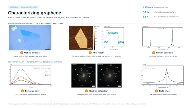
- MeasureSweep the gate: the resistance peaks at the Dirac point. On 300 nm SiO₂ each volt adds 7.2 × 10¹⁰ carriers per cm²; the first devices held electrons or holes up to 10¹³ cm⁻² with room-temperature mobilities of about 10,000 cm²/V·s (Novoselov et al. 2004). Fitting R = R_c + (L/W)/(eμ√(n₀² + n²)) gives the mobility and the residual density (Kim et al. 2009)
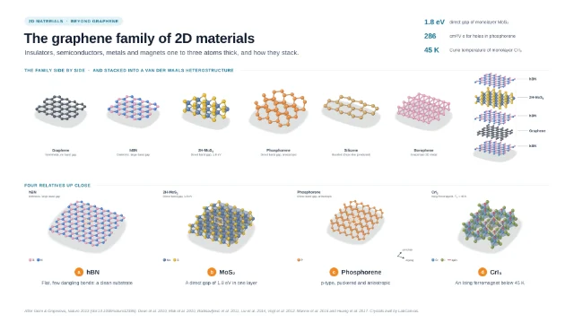
- Cleaner devicesOn hBN, mobilities and carrier inhomogeneity are almost an order of magnitude better than on SiO₂ (Dean et al. 2010); hBN/graphene/hBN stacks contacted along their one-dimensional edge carry ballistic transport over more than 15 µm at low temperature (Wang et al. 2013)
Strengths
- Standard cleanroom steps: photolithography, oxygen-plasma etching, evaporation and lift-off (Kuzum et al. 2014)
- The doped silicon substrate doubles as the gate
Limitations
- Graphene on SiO₂ is highly disordered compared with graphene on hBN (Dean et al. 2010)
- Each pattern needs its own resist step and alignment
Uses
- Field-effect transistors
- Hall and quantum Hall measurements
- Transparent electrodes for neural recording (Kuzum et al. 2014)
Papers this template follows
- Novoselov et al., “Electric field effect in atomically thin carbon films”, Science 2004. doi:10.1126/science.1102896primary
- Kim et al., “Realization of a high mobility dual-gated graphene field-effect transistor with Al2O3 dielectric”, Appl. Phys. Lett. 2009. doi:10.1063/1.3077021primary
- Kuzum et al., “Transparent and flexible low noise graphene electrodes for simultaneous electrophysiology and neuroimaging”, Nat. Commun. 2014. doi:10.1038/ncomms6259method origin
- Dean et al., “Boron nitride substrates for high-quality graphene electronics”, Nat. Nanotechnol. 2010. doi:10.1038/nnano.2010.172further reading
- Wang et al., “One-dimensional electrical contact to a two-dimensional material”, Science 2013. doi:10.1126/science.1244358further reading
After Novoselov et al., Science 2004 (doi:10.1126/science.1102896), Kim et al., APL 2009, Kuzum et al., Nat. Commun. 2014, Dean et al., Nat. Nanotechnol. 2010 and Wang et al., Science 2013. Transfer curve computed; contact resistance and residual density illustrative.
How templates are written and checked: editorial guidelines.
Questions
What does the “Making a graphene transistor” template show?
A graphene field-effect transistor is made with two rounds of lithography: the first patterns the graphene into a channel with an oxygen plasma, the second adds Cr/Au contacts by lift-off. The doped silicon under the oxide is the gate, and the resistance against gate voltage gives the Dirac point, the carrier density and the mobility.
What are the steps shown in “Making a graphene transistor”?
1. Pattern the graphene: Spin-coat resist, expose it through a photomask (or write it with an electron beam), develop, remove the uncovered graphene in an oxygen plasma and strip the resist. 2. Make the contacts: Pattern a second resist layer, evaporate Cr/Au and lift off the metal on the resist (Kuzum et al. 2014 used 10 nm Cr and 100 nm Au). 3. Gate and bond: The doped silicon under the SiO₂ is the back gate; bond wires connect the pads to the measurement. 4. Measure: Sweep the gate: the resistance peaks at the Dirac point. On 300 nm SiO₂ each volt adds 7.2 × 10¹⁰ carriers per cm²; the first devices held electrons or holes up to 10¹³ cm⁻² with room-temperature mobilities of about 10,000 cm²/V·s (Novoselov et al. 2004). Fitting R = R_c + (L/W)/(eμ√(n₀² + n²)) gives the mobility and the residual density (Kim et al. 2009). 5. Cleaner devices: On hBN, mobilities and carrier inhomogeneity are almost an order of magnitude better than on SiO₂ (Dean et al. 2010); hBN/graphene/hBN stacks contacted along their one-dimensional edge carry ballistic transport over more than 15 µm at low temperature (Wang et al. 2013).
What are the starting materials and the product?
Starting materials: Graphene on SiO₂/Si (exfoliated, or CVD-grown and transferred). Product: A Hall bar or two-terminal field-effect device with Cr/Au contacts, gated through the oxide.
Which papers is “Making a graphene transistor” based on?
Novoselov et al., “Electric field effect in atomically thin carbon films”, Science 2004 (doi:10.1126/science.1102896); Kim et al., “Realization of a high mobility dual-gated graphene field-effect transistor with Al2O3 dielectric”, Appl. Phys. Lett. 2009 (doi:10.1063/1.3077021); Kuzum et al., “Transparent and flexible low noise graphene electrodes for simultaneous electrophysiology and neuroimaging”, Nat. Commun. 2014 (doi:10.1038/ncomms6259); Dean et al., “Boron nitride substrates for high-quality graphene electronics”, Nat. Nanotechnol. 2010 (doi:10.1038/nnano.2010.172); Wang et al., “One-dimensional electrical contact to a two-dimensional material”, Science 2013 (doi:10.1126/science.1244358).
Can I edit the “Making a graphene transistor” template?
Yes. Open it in the LabCanvas editor: all 36 layers are editable, including 5 generated objects (structures, plots, equipment) with their own settings. Change the text, colours and layout, then export PNG, TIFF, SVG or PDF.
Do I need an account to use this template?
Not to view it here. To open and edit it, sign in to LabCanvas or create a free account (the free plan keeps up to 3 designs). Downloading the figure is part of LabCanvas Pro (US$19 a month or US$199 a year).