Graphical abstract template · Graphene research · Defects and doping
Defects and doping in graphene
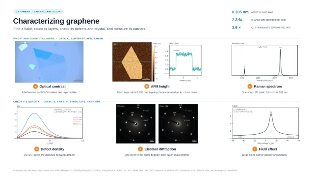
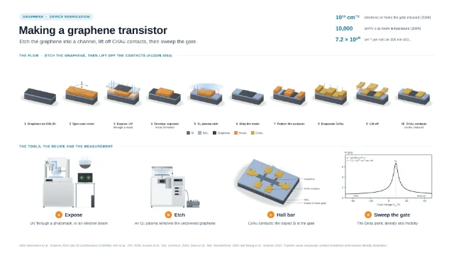
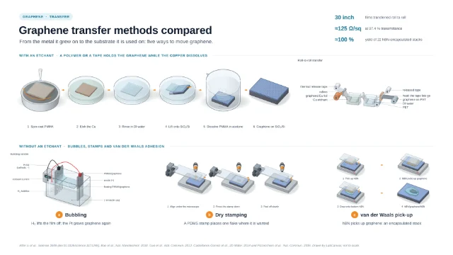
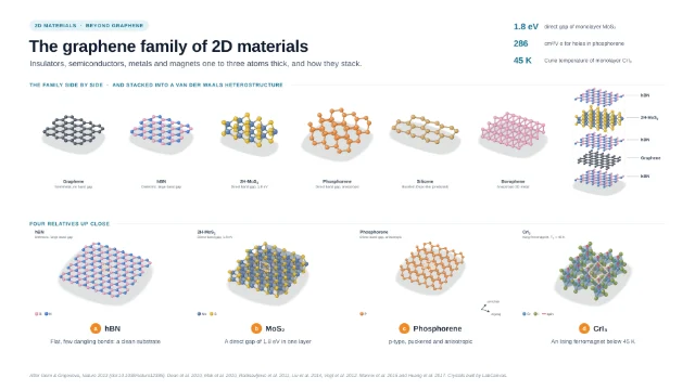
Defects and dopants in graphene in six panels: the Stone–Wales defect, a single vacancy, a grain boundary of 5-7 pairs, the nitrogen sites of N-doped graphene, transfer curves whose Dirac point shifts with doping, and the N 1s XPS that tells the nitrogen sites apart.
Updated 11 cited papers45 editable layers

At a glance
- Category
- Graphene research
- Method
- Defects and doping
- Starting materials
- Graphene, CVD graphene with grain boundaries, N-doped graphene
- Product
- Defect structures, dopant sites and their signatures in transport and XPS
- Key result
- Defects built on the lattice and relaxed; curves and spectra computed by LabCanvas from the cited values; relaxed coordinates and the two Dirac-point voltages are drawing choices
- Figure
- 1920 × 1080 px (16:9), 45 editable layers, 6 generated objects
Step by step
- Stone–WalesThe 55-77 defect: a bond turned by 90° (Kotakoski et al. 2011)
- VacanciesThe 5-9 single vacancy and its dangling bond (Zhou et al. 2022); the 5-8-5 and 555-777 divacancies (Lee et al. 2005)
- Grain boundariesA symmetric tilt boundary of 5-7 pairs, as in polycrystalline CVD graphene (Huang et al. 2011)
- Nitrogen sitesGraphitic N, pyridinic N at an edge and around a vacancy, pyrrolic N in a five-membered ring with N–H, and pyridinic N-oxide (Zhang et al. 2016; Chuang et al. 2017; Pels et al. 1995)
- Dirac point shiftsThe transfer curve R(V_g) peaks at the Dirac point V_D; the carriers are n = C_g(V_g − V_D)/e, so doping moves the peak (Novoselov et al. 2004; Kim et al. 2009)
- N 1s XPSN-doped graphene annealed in NH₃ at 600 °C: pyridinic 398.8–398.9, pyrrolic 400.3–400.4 and graphitic 401.8–401.9 eV (Huang et al. 2026)
Strengths
- Each defect has a distinct ring pattern
- Dopants tune the carriers and the chemistry
- XPS separates the nitrogen sites
Limitations
- Real samples mix several defect types
- Binding energies vary between studies
Uses
- Explaining Raman D bands and mobility loss
- Catalysis on N-doped graphene
- Chemical doping of devices
Papers this template follows
- Banhart, Kotakoski & Krasheninnikov, “Structural defects in graphene”, ACS Nano 2011. doi:10.1021/nn102598mprimary
- Kotakoski et al., “Stone-Wales-type transformations in carbon nanostructures driven by electron irradiation”, Phys. Rev. B 2011. doi:10.1103/PhysRevB.83.245420primary
- Huang et al., “Grains and grain boundaries in single-layer graphene atomic patchwork quilts”, Nature 2011. doi:10.1038/nature09718primary
- Zhang et al., “Tunable electronic properties of graphene through controlling bonding configurations of doped nitrogen atoms”, Sci. Rep. 2016. doi:10.1038/srep28330primary
- Huang et al., “Nitrogen-doped graphene with enhanced room temperature NH₃ gas sensing properties”, Nanomaterials 2026. doi:10.3390/nano16161044primary
- Zhou, Mallia & Harrison, “Strain-tuneable magnetism and spintronics of distorted monovacancies in graphene”, J. Phys. Chem. C 2022. doi:10.1021/acs.jpcc.2c05494further reading
- Lee et al., “Diffusion, coalescence, and reconstruction of vacancy defects in graphene layers”, Phys. Rev. Lett. 2005. doi:10.1103/PhysRevLett.95.205501further reading
- Chuang et al., “Chemical modification of graphene oxide by nitrogenation: an X-ray absorption and emission spectroscopy study”, Sci. Rep. 2017. doi:10.1038/srep42235further reading
- Pels et al., “Evolution of nitrogen functionalities in carbonaceous materials during pyrolysis”, Carbon 1995. doi:10.1016/0008-6223(95)00154-6further reading
- Novoselov et al., “Electric field effect in atomically thin carbon films”, Science 2004. doi:10.1126/science.1102896further reading
- Kim et al., “Realization of a high mobility dual-gated graphene field-effect transistor with Al2O3 dielectric”, Appl. Phys. Lett. 2009. doi:10.1063/1.3077021further reading
Computed by LabCanvas after Banhart, Kotakoski & Krasheninnikov, ACS Nano 2011 (doi:10.1021/nn102598m), Kotakoski et al., PRB 2011, Huang et al., Nature 2011, Zhang et al., Sci. Rep. 2016, Huang et al., Nanomaterials 2026, and the papers in the details.
How templates are written and checked: editorial guidelines.
Questions
What does the “Defects and doping in graphene” template show?
Defects and dopants in graphene in six panels: the Stone–Wales defect, a single vacancy, a grain boundary of 5-7 pairs, the nitrogen sites of N-doped graphene, transfer curves whose Dirac point shifts with doping, and the N 1s XPS that tells the nitrogen sites apart.
What are the steps shown in “Defects and doping in graphene”?
1. Stone–Wales: The 55-77 defect: a bond turned by 90° (Kotakoski et al. 2011). 2. Vacancies: The 5-9 single vacancy and its dangling bond (Zhou et al. 2022); the 5-8-5 and 555-777 divacancies (Lee et al. 2005). 3. Grain boundaries: A symmetric tilt boundary of 5-7 pairs, as in polycrystalline CVD graphene (Huang et al. 2011). 4. Nitrogen sites: Graphitic N, pyridinic N at an edge and around a vacancy, pyrrolic N in a five-membered ring with N–H, and pyridinic N-oxide (Zhang et al. 2016; Chuang et al. 2017; Pels et al. 1995). 5. Dirac point shifts: The transfer curve R(V_g) peaks at the Dirac point V_D; the carriers are n = C_g(V_g − V_D)/e, so doping moves the peak (Novoselov et al. 2004; Kim et al. 2009). 6. N 1s XPS: N-doped graphene annealed in NH₃ at 600 °C: pyridinic 398.8–398.9, pyrrolic 400.3–400.4 and graphitic 401.8–401.9 eV (Huang et al. 2026).
What are the starting materials and the product?
Starting materials: Graphene, CVD graphene with grain boundaries, N-doped graphene. Product: Defect structures, dopant sites and their signatures in transport and XPS.
Which papers is “Defects and doping in graphene” based on?
Banhart, Kotakoski & Krasheninnikov, “Structural defects in graphene”, ACS Nano 2011 (doi:10.1021/nn102598m); Kotakoski et al., “Stone-Wales-type transformations in carbon nanostructures driven by electron irradiation”, Phys. Rev. B 2011 (doi:10.1103/PhysRevB.83.245420); Huang et al., “Grains and grain boundaries in single-layer graphene atomic patchwork quilts”, Nature 2011 (doi:10.1038/nature09718); Zhang et al., “Tunable electronic properties of graphene through controlling bonding configurations of doped nitrogen atoms”, Sci. Rep. 2016 (doi:10.1038/srep28330); Huang et al., “Nitrogen-doped graphene with enhanced room temperature NH₃ gas sensing properties”, Nanomaterials 2026 (doi:10.3390/nano16161044); Zhou, Mallia & Harrison, “Strain-tuneable magnetism and spintronics of distorted monovacancies in graphene”, J. Phys. Chem. C 2022 (doi:10.1021/acs.jpcc.2c05494); Lee et al., “Diffusion, coalescence, and reconstruction of vacancy defects in graphene layers”, Phys. Rev. Lett. 2005 (doi:10.1103/PhysRevLett.95.205501); Chuang et al., “Chemical modification of graphene oxide by nitrogenation: an X-ray absorption and emission spectroscopy study”, Sci. Rep. 2017 (doi:10.1038/srep42235); Pels et al., “Evolution of nitrogen functionalities in carbonaceous materials during pyrolysis”, Carbon 1995 (doi:10.1016/0008-6223(95)00154-6); Novoselov et al., “Electric field effect in atomically thin carbon films”, Science 2004 (doi:10.1126/science.1102896); Kim et al., “Realization of a high mobility dual-gated graphene field-effect transistor with Al2O3 dielectric”, Appl. Phys. Lett. 2009 (doi:10.1063/1.3077021).
Can I edit the “Defects and doping in graphene” template?
Yes. Open it in the LabCanvas editor: all 45 layers are editable, including 6 generated objects (structures, plots, equipment) with their own settings. Change the text, colours and layout, then export PNG, TIFF, SVG or PDF.
Do I need an account to use this template?
Not to view it here. To open and edit it, sign in to LabCanvas or create a free account (the free plan keeps up to 3 designs). Downloading the figure is part of LabCanvas Pro (US$19 a month or US$199 a year).