Graphical abstract template · Graphene research · Electronics
Graphene electronics
Graphene devices in six panels: a Hall bar on SiO₂/Si, an hBN-encapsulated device with edge contacts, the field-effect transfer curve, RF transistors with an f_T benchmark, a suspended mechanical resonator, and the quantum Hall resistance standard on epitaxial graphene.
Updated 11 cited papers45 editable layers

At a glance
- Category
- Graphene research
- Method
- Electronics
- Starting materials
- Exfoliated graphene on SiO₂/Si or in hBN, epitaxial graphene on SiC
- Product
- Transistors, resonators and quantum resistance standards
- Key result
- Devices drawn in 3D after the cited papers, heights exaggerated; curves computed from the cited models; the resonator’s quality factor and the field axis of the plateaus are settings without numbers
- Figure
- 1920 × 1080 px (16:9), 45 editable layers, 6 generated objects
Step by step
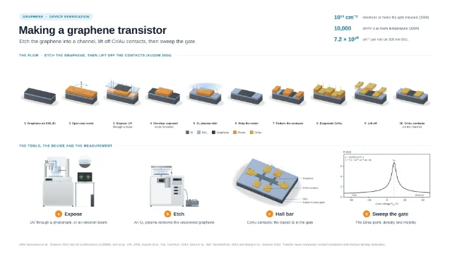
- Hall barGraphene on SiO₂ over doped Si as the back gate (Novoselov et al. 2004); current through the end contacts, V_xx measured along the channel and V_xy across it
- Encapsulated, edge-contactedhBN/graphene/hBN stacks contacted by metal along the one-dimensional edge (Wang et al. 2013); hBN as a substrate for high-quality graphene (Dean et al. 2010)
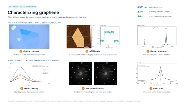
- Field effectThe resistance peaks at the Dirac point; on 300 nm SiO₂ each volt on the gate adds 7.2 × 10¹⁰ carriers per cm², and the first devices reached about 10,000 cm²/V·s at room temperature (Novoselov et al. 2004)
- RF transistorsOn epitaxial graphene on the Si face of SiC, a cutoff frequency of 100 GHz for a gate length of 240 nm (Lin et al. 2010); f_T is the unity-current-gain frequency (Petrone et al. 2013)
- ResonatorsSingle- and multilayer sheets exfoliated over trenches in silicon oxide vibrate at fundamental frequencies in the MHz range, actuated optically or electrically and read out by interferometry (Bunch et al. 2007)
- Resistance standardMonolayer epitaxial graphene quantized the Hall resistance to 3 parts per billion at 300 mK (Tzalenchuk et al. 2010); on epitaxial graphene only ν = 2, 6, 10 appear and only the ν = 2 plateau, R_K/2 ≈ 12 906 Ω, is fully quantized (Panna et al. 2021; Liu et al. 2020)
Strengths
- The gate tunes graphene from holes to electrons
- High-frequency operation on wafer-scale SiC (Lin et al. 2010)
- A resistance standard from a single material (Tzalenchuk et al. 2010)
Limitations
- No band gap: transistors do not switch off
- Contacts and substrates limit the mobility
Uses
- RF amplifiers and mixers
- Mass and charge sensing
- Electrical metrology
Papers this template follows
- Novoselov et al., “Electric field effect in atomically thin carbon films”, Science 2004. doi:10.1126/science.1102896primary
- Wang et al., “One-dimensional electrical contact to a two-dimensional material”, Science 2013. doi:10.1126/science.1244358primary
- Lin et al., “100-GHz transistors from wafer-scale epitaxial graphene”, Science 2010. doi:10.1126/science.1184289primary
- Bunch et al., “Electromechanical resonators from graphene sheets”, Science 2007. doi:10.1126/science.1136836primary
- Tzalenchuk et al., “Towards a quantum resistance standard based on epitaxial graphene”, Nat. Nanotechnol. 2010. doi:10.1038/nnano.2009.474primary
- Dean et al., “Boron nitride substrates for high-quality graphene electronics”, Nat. Nanotechnol. 2010. doi:10.1038/nnano.2010.172further reading
- Petrone et al., “Graphene field-effect transistors with gigahertz-frequency power gain on flexible substrates”, Nano Lett. 2013. doi:10.1021/nl303666mfurther reading
- Liao et al., “High-speed graphene transistors with a self-aligned nanowire gate”, Nature 2010. doi:10.1038/nature09405further reading
- Panna et al., “Graphene quantum Hall effect parallel resistance arrays”, Phys. Rev. B 2021. doi:10.1103/physrevb.103.075408further reading
- Liu et al., “Analysing quantized resistance behaviour in graphene Corbino p-n junction devices”, J. Phys. D 2020. doi:10.1088/1361-6463/ab83bbfurther reading
- Kim et al., “Realization of a high mobility dual-gated graphene field-effect transistor with Al2O3 dielectric”, Appl. Phys. Lett. 2009. doi:10.1063/1.3077021further reading
Drawn and computed by LabCanvas after Novoselov et al., Science 2004 (doi:10.1126/science.1102896), Wang et al., Science 2013, Lin et al., Science 2010, Bunch et al., Science 2007, Tzalenchuk et al., Nat. Nanotechnol. 2010, and the papers in the details.
How templates are written and checked: editorial guidelines.
Questions
What does the “Graphene electronics” template show?
Graphene devices in six panels: a Hall bar on SiO₂/Si, an hBN-encapsulated device with edge contacts, the field-effect transfer curve, RF transistors with an f_T benchmark, a suspended mechanical resonator, and the quantum Hall resistance standard on epitaxial graphene.
What are the steps shown in “Graphene electronics”?
1. Hall bar: Graphene on SiO₂ over doped Si as the back gate (Novoselov et al. 2004); current through the end contacts, V_xx measured along the channel and V_xy across it. 2. Encapsulated, edge-contacted: hBN/graphene/hBN stacks contacted by metal along the one-dimensional edge (Wang et al. 2013); hBN as a substrate for high-quality graphene (Dean et al. 2010). 3. Field effect: The resistance peaks at the Dirac point; on 300 nm SiO₂ each volt on the gate adds 7.2 × 10¹⁰ carriers per cm², and the first devices reached about 10,000 cm²/V·s at room temperature (Novoselov et al. 2004). 4. RF transistors: On epitaxial graphene on the Si face of SiC, a cutoff frequency of 100 GHz for a gate length of 240 nm (Lin et al. 2010); f_T is the unity-current-gain frequency (Petrone et al. 2013). 5. Resonators: Single- and multilayer sheets exfoliated over trenches in silicon oxide vibrate at fundamental frequencies in the MHz range, actuated optically or electrically and read out by interferometry (Bunch et al. 2007). 6. Resistance standard: Monolayer epitaxial graphene quantized the Hall resistance to 3 parts per billion at 300 mK (Tzalenchuk et al. 2010); on epitaxial graphene only ν = 2, 6, 10 appear and only the ν = 2 plateau, R_K/2 ≈ 12 906 Ω, is fully quantized (Panna et al. 2021; Liu et al. 2020).
What are the starting materials and the product?
Starting materials: Exfoliated graphene on SiO₂/Si or in hBN, epitaxial graphene on SiC. Product: Transistors, resonators and quantum resistance standards.
Which papers is “Graphene electronics” based on?
Novoselov et al., “Electric field effect in atomically thin carbon films”, Science 2004 (doi:10.1126/science.1102896); Wang et al., “One-dimensional electrical contact to a two-dimensional material”, Science 2013 (doi:10.1126/science.1244358); Lin et al., “100-GHz transistors from wafer-scale epitaxial graphene”, Science 2010 (doi:10.1126/science.1184289); Bunch et al., “Electromechanical resonators from graphene sheets”, Science 2007 (doi:10.1126/science.1136836); Tzalenchuk et al., “Towards a quantum resistance standard based on epitaxial graphene”, Nat. Nanotechnol. 2010 (doi:10.1038/nnano.2009.474); Dean et al., “Boron nitride substrates for high-quality graphene electronics”, Nat. Nanotechnol. 2010 (doi:10.1038/nnano.2010.172); Petrone et al., “Graphene field-effect transistors with gigahertz-frequency power gain on flexible substrates”, Nano Lett. 2013 (doi:10.1021/nl303666m); Liao et al., “High-speed graphene transistors with a self-aligned nanowire gate”, Nature 2010 (doi:10.1038/nature09405); Panna et al., “Graphene quantum Hall effect parallel resistance arrays”, Phys. Rev. B 2021 (doi:10.1103/physrevb.103.075408); Liu et al., “Analysing quantized resistance behaviour in graphene Corbino p-n junction devices”, J. Phys. D 2020 (doi:10.1088/1361-6463/ab83bb); Kim et al., “Realization of a high mobility dual-gated graphene field-effect transistor with Al2O3 dielectric”, Appl. Phys. Lett. 2009 (doi:10.1063/1.3077021).
Can I edit the “Graphene electronics” template?
Yes. Open it in the LabCanvas editor: all 45 layers are editable, including 6 generated objects (structures, plots, equipment) with their own settings. Change the text, colours and layout, then export PNG, TIFF, SVG or PDF.
Do I need an account to use this template?
Not to view it here. To open and edit it, sign in to LabCanvas or create a free account (the free plan keeps up to 3 designs). Downloading the figure is part of LabCanvas Pro (US$19 a month or US$199 a year).