Graphical abstract template · Graphene research · Scale-up and QC
Graphene scale-up and quality control
Graphene manufacturing in six panels: roll-to-roll CVD in a concentric-tube reactor, a roll-to-roll transfer line onto PET, metre-sized single crystals on industrial Cu foil, THz sheet-conductance and Raman quality maps, and the framework that classifies graphene-based materials.
Updated 10 cited papers45 editable layers

At a glance
- Category
- Graphene research
- Method
- Scale-up and QC
- Starting materials
- Cu foil, methane and hydrogen; CVD graphene films
- Product
- Graphene films by the metre, quality maps and a material classification
- Key result
- Machines drawn in 3D after the cited papers, lengths compressed; map patterns are seeded noise scaled to the reported means and spreads
- Figure
- 1920 × 1080 px (16:9), 45 editable layers, 6 generated objects
Step by step
- Roll-to-roll CVDA 0.25-inch Cu foil wound 1.5 turns round a 13 mm quartz tube moves through the 4.5 mm gap inside a 25 mm tube; annealed in H₂, then grown in CH₄/H₂ at 1010 °C and 4 Torr, at 25–500 mm/min (Polsen et al. 2015)
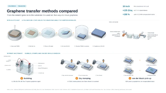
- Roll-to-roll transferThermal release tape, through a Cu etchant and a rinse, released onto PET by hot rollers and doped wet-chemically (Bae et al. 2010); the tape holds firmly at room temperature and lets go when heated (Woo 2019)
- Single crystalsTemperature-gradient annealing turned industrial polycrystalline Cu foil into metre-sized single-crystal Cu(111); a 5 × 50 cm film grew in 20 min (Xu et al. 2017)
- THz conductance mapSheet conductance of 10 × 10 mm chips of CVD graphene mapped contactless by THz time-domain spectroscopy (Melios et al. 2020; Cultrera et al. 2019)
- Raman mapThe 2D width and I(2D)/I(G) mapped against the NPL criteria, ≤ 35 cm⁻¹ and ≥ 2: 26.2 ± 1.7 cm⁻¹ and 2.4 ± 0.7 over 32 × 32 µm of CVD graphene on Si/SiO₂ at 532 nm (Muñoz-Vargas et al. 2025)
- What kind of grapheneGraphene-based materials classified by number of layers, average lateral size and atomic C/O ratio (Wick et al. 2014); few-layer graphene has 3 to 10 layers and nanoplatelets are 100 nm to 100 µm across (ISO/TS 80004-13, as Nicoletti et al. 2024 quote it)
Strengths
- Continuous growth and transfer by the metre (Polsen et al. 2015; Bae et al. 2010)
- Contactless, wafer-scale mapping (Melios et al. 2020)
- A shared vocabulary for products (Wick et al. 2014)
Limitations
- At high speed domains have no time to coalesce (Polsen et al. 2015)
- THz maps are affected about 1 mm from an edge (Melios et al. 2020)
Uses
- Industrial graphene films
- Incoming inspection of graphene products
- Specifications and standards
Papers this template follows
- Polsen et al., “High-speed roll-to-roll manufacturing of graphene using a concentric tube CVD reactor”, Sci. Rep. 2015. doi:10.1038/srep10257primary
- Bae et al., “Roll-to-roll production of 30-inch graphene films for transparent electrodes”, Nat. Nanotechnol. 2010. doi:10.1038/nnano.2010.132primary
- Xu et al., “Ultrafast epitaxial growth of metre-sized single-crystal graphene on industrial Cu foil”, Sci. Bull. 2017. doi:10.1016/j.scib.2017.07.005primary
- Melios et al., “Towards standardisation of contact and contactless electrical measurements of CVD graphene at the macro-, micro- and nano-scale”, Sci. Rep. 2020. doi:10.1038/s41598-020-59851-1primary
- Muñoz-Vargas et al., “Simple graphene film production by chemical vapour deposition and the use of AI for quality analysis”, Nanoscale Adv. 2025. doi:10.1039/d5na00668fprimary
- Wick et al., “Classification framework for graphene-based materials”, Angew. Chem. Int. Ed. 2014. doi:10.1002/anie.201403335primary
- Woo, “Transparent conductive electrodes based on graphene-related materials”, Micromachines 2019. doi:10.3390/mi10010013further reading
- Cultrera et al., “Mapping the conductivity of graphene with electrical resistance tomography”, Sci. Rep. 2019. doi:10.1038/s41598-019-46713-8further reading
- Nicoletti et al., “Non-cytotoxic graphene nanoplatelets upregulate cell proliferation and self-renewal genes of mesenchymal stem cells”, Int. J. Mol. Sci. 2024. doi:10.3390/ijms25189817further reading
- Kidambi et al., “A scalable route to nanoporous large-area atomically thin graphene membranes by roll-to-roll chemical vapor deposition and polymer support casting”, ACS Appl. Mater. Interfaces 2018. doi:10.1021/acsami.8b00846further reading
Drawn and computed by LabCanvas after Polsen et al., Sci. Rep. 2015 (doi:10.1038/srep10257), Bae et al., Nat. Nanotechnol. 2010, Xu et al., Sci. Bull. 2017, Melios et al., Sci. Rep. 2020, Muñoz-Vargas et al., Nanoscale Adv. 2025, Wick et al., Angew. Chem. 2014, and the papers in the details.
How templates are written and checked: editorial guidelines.
Questions
What does the “Graphene scale-up and quality control” template show?
Graphene manufacturing in six panels: roll-to-roll CVD in a concentric-tube reactor, a roll-to-roll transfer line onto PET, metre-sized single crystals on industrial Cu foil, THz sheet-conductance and Raman quality maps, and the framework that classifies graphene-based materials.
What are the steps shown in “Graphene scale-up and quality control”?
1. Roll-to-roll CVD: A 0.25-inch Cu foil wound 1.5 turns round a 13 mm quartz tube moves through the 4.5 mm gap inside a 25 mm tube; annealed in H₂, then grown in CH₄/H₂ at 1010 °C and 4 Torr, at 25–500 mm/min (Polsen et al. 2015). 2. Roll-to-roll transfer: Thermal release tape, through a Cu etchant and a rinse, released onto PET by hot rollers and doped wet-chemically (Bae et al. 2010); the tape holds firmly at room temperature and lets go when heated (Woo 2019). 3. Single crystals: Temperature-gradient annealing turned industrial polycrystalline Cu foil into metre-sized single-crystal Cu(111); a 5 × 50 cm film grew in 20 min (Xu et al. 2017). 4. THz conductance map: Sheet conductance of 10 × 10 mm chips of CVD graphene mapped contactless by THz time-domain spectroscopy (Melios et al. 2020; Cultrera et al. 2019). 5. Raman map: The 2D width and I(2D)/I(G) mapped against the NPL criteria, ≤ 35 cm⁻¹ and ≥ 2: 26.2 ± 1.7 cm⁻¹ and 2.4 ± 0.7 over 32 × 32 µm of CVD graphene on Si/SiO₂ at 532 nm (Muñoz-Vargas et al. 2025). 6. What kind of graphene: Graphene-based materials classified by number of layers, average lateral size and atomic C/O ratio (Wick et al. 2014); few-layer graphene has 3 to 10 layers and nanoplatelets are 100 nm to 100 µm across (ISO/TS 80004-13, as Nicoletti et al. 2024 quote it).
What are the starting materials and the product?
Starting materials: Cu foil, methane and hydrogen; CVD graphene films. Product: Graphene films by the metre, quality maps and a material classification.
Which papers is “Graphene scale-up and quality control” based on?
Polsen et al., “High-speed roll-to-roll manufacturing of graphene using a concentric tube CVD reactor”, Sci. Rep. 2015 (doi:10.1038/srep10257); Bae et al., “Roll-to-roll production of 30-inch graphene films for transparent electrodes”, Nat. Nanotechnol. 2010 (doi:10.1038/nnano.2010.132); Xu et al., “Ultrafast epitaxial growth of metre-sized single-crystal graphene on industrial Cu foil”, Sci. Bull. 2017 (doi:10.1016/j.scib.2017.07.005); Melios et al., “Towards standardisation of contact and contactless electrical measurements of CVD graphene at the macro-, micro- and nano-scale”, Sci. Rep. 2020 (doi:10.1038/s41598-020-59851-1); Muñoz-Vargas et al., “Simple graphene film production by chemical vapour deposition and the use of AI for quality analysis”, Nanoscale Adv. 2025 (doi:10.1039/d5na00668f); Wick et al., “Classification framework for graphene-based materials”, Angew. Chem. Int. Ed. 2014 (doi:10.1002/anie.201403335); Woo, “Transparent conductive electrodes based on graphene-related materials”, Micromachines 2019 (doi:10.3390/mi10010013); Cultrera et al., “Mapping the conductivity of graphene with electrical resistance tomography”, Sci. Rep. 2019 (doi:10.1038/s41598-019-46713-8); Nicoletti et al., “Non-cytotoxic graphene nanoplatelets upregulate cell proliferation and self-renewal genes of mesenchymal stem cells”, Int. J. Mol. Sci. 2024 (doi:10.3390/ijms25189817); Kidambi et al., “A scalable route to nanoporous large-area atomically thin graphene membranes by roll-to-roll chemical vapor deposition and polymer support casting”, ACS Appl. Mater. Interfaces 2018 (doi:10.1021/acsami.8b00846).
Can I edit the “Graphene scale-up and quality control” template?
Yes. Open it in the LabCanvas editor: all 45 layers are editable, including 6 generated objects (structures, plots, equipment) with their own settings. Change the text, colours and layout, then export PNG, TIFF, SVG or PDF.
Do I need an account to use this template?
Not to view it here. To open and edit it, sign in to LabCanvas or create a free account (the free plan keeps up to 3 designs). Downloading the figure is part of LabCanvas Pro (US$19 a month or US$199 a year).