Graphical abstract template · Graphene research · Sensors
Graphene sensors and optoelectronics
Graphene sensing and optoelectronics in six panels: single NO₂ molecules detected as resistance steps, a metal–graphene–metal photodetector and its frequency response, a flexible transparent electrode and transparent neural electrodes that neurons are imaged through.
Updated 9 cited papers45 editable layers

At a glance
- Category
- Graphene research
- Method
- Sensors
- Starting materials
- Exfoliated and CVD graphene on SiO₂/Si or PET
- Product
- Gas sensors, photodetectors and transparent electrodes
- Key result
- Devices drawn in 3D after the cited papers, heights exaggerated; resistance steps and frequency response computed from the cited values
- Figure
- 1920 × 1080 px (16:9), 45 editable layers, 6 generated objects
Step by step
- Single-molecule sensorMicrometre-size graphene sensors detect single gas molecules: each one that attaches or detaches changes the local carrier concentration by one electron (Schedin et al. 2007); NO₂ is a strong acceptor, its dimer N₂O₄ dopes only weakly (Wehling et al. 2008)
- Resistance stepsEach attachment or detachment is a step in the resistance; graphene is exceptionally low in noise (Schedin et al. 2007); resist residue dopes graphene and concentrates analyte (Dan et al. 2009)
- PhotodetectorGraphene on SiO₂ over a Si back gate with Ti/Au contacts; at the metal–graphene junction the local field separates electrons and holes, so it works without a source–drain bias (Xia et al. 2009; Park et al. 2009)
- How fastNo degradation up to 40 GHz (Xia et al. 2009); an intrinsic response time of 2.1 ps, a bandwidth of ≈ 262 GHz (Urich et al. 2011)
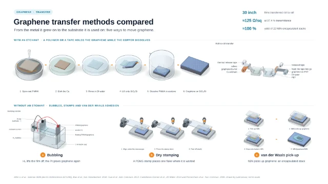
- Transparent electrodeRoll-to-roll, predominantly monolayer 30-inch CVD films: sheet resistance as low as ≈ 125 Ω/sq at 97.4 % transmittance; doped four-layer films ≈ 30 Ω/sq at ≈ 90 % (Bae et al. 2010)
- See through the electrodeNeurons in hippocampal slices were imaged through transparent graphene electrodes by confocal and two-photon microscopy with no light-induced artefacts in the recordings (Kuzum et al. 2014)
Strengths
- Every atom is on the surface
- Fast, unbiased photodetection (Xia et al. 2009)
- Transparent and flexible (Bae et al. 2010)
Limitations
- Residues and substrates change the response (Dan et al. 2009)
- About 2 % absorption limits the responsivity (Xia et al. 2009)
Uses
- Gas and chemical sensors
- Optical communications
- Touch screens and bioelectronics
Papers this template follows
- Schedin et al., “Detection of individual gas molecules adsorbed on graphene”, Nat. Mater. 2007. doi:10.1038/nmat1967primary
- Xia et al., “Ultrafast graphene photodetector”, Nat. Nanotechnol. 2009. doi:10.1038/nnano.2009.292primary
- Urich, Unterrainer & Mueller, “Intrinsic response time of graphene photodetectors”, Nano Lett. 2011. doi:10.1021/nl2011388primary
- Bae et al., “Roll-to-roll production of 30-inch graphene films for transparent electrodes”, Nat. Nanotechnol. 2010. doi:10.1038/nnano.2010.132primary
- Kuzum et al., “Transparent and flexible low noise graphene electrodes for simultaneous electrophysiology and neuroimaging”, Nat. Commun. 2014. doi:10.1038/ncomms6259primary
- Wehling et al., “Molecular doping of graphene”, Nano Lett. 2008. doi:10.1021/nl072364wfurther reading
- Dan et al., “Intrinsic response of graphene vapor sensors”, Nano Lett. 2009. doi:10.1021/nl8033637further reading
- Park, Ahn & Ruiz-Vargas, “Imaging of photocurrent generation and collection in single-layer graphene”, Nano Lett. 2009. doi:10.1021/nl8029493further reading
- Echtermeyer et al., “Surface plasmon polariton graphene photodetectors”, Nano Lett. 2016. doi:10.1021/acs.nanolett.5b02051further reading
Drawn and computed by LabCanvas after Schedin et al., Nat. Mater. 2007 (doi:10.1038/nmat1967), Xia et al., Nat. Nanotechnol. 2009, Urich et al., Nano Lett. 2011, Bae et al., Nat. Nanotechnol. 2010, Kuzum et al., Nat. Commun. 2014, and the papers in the details.
How templates are written and checked: editorial guidelines.
Questions
What does the “Graphene sensors and optoelectronics” template show?
Graphene sensing and optoelectronics in six panels: single NO₂ molecules detected as resistance steps, a metal–graphene–metal photodetector and its frequency response, a flexible transparent electrode and transparent neural electrodes that neurons are imaged through.
What are the steps shown in “Graphene sensors and optoelectronics”?
1. Single-molecule sensor: Micrometre-size graphene sensors detect single gas molecules: each one that attaches or detaches changes the local carrier concentration by one electron (Schedin et al. 2007); NO₂ is a strong acceptor, its dimer N₂O₄ dopes only weakly (Wehling et al. 2008). 2. Resistance steps: Each attachment or detachment is a step in the resistance; graphene is exceptionally low in noise (Schedin et al. 2007); resist residue dopes graphene and concentrates analyte (Dan et al. 2009). 3. Photodetector: Graphene on SiO₂ over a Si back gate with Ti/Au contacts; at the metal–graphene junction the local field separates electrons and holes, so it works without a source–drain bias (Xia et al. 2009; Park et al. 2009). 4. How fast: No degradation up to 40 GHz (Xia et al. 2009); an intrinsic response time of 2.1 ps, a bandwidth of ≈ 262 GHz (Urich et al. 2011). 5. Transparent electrode: Roll-to-roll, predominantly monolayer 30-inch CVD films: sheet resistance as low as ≈ 125 Ω/sq at 97.4 % transmittance; doped four-layer films ≈ 30 Ω/sq at ≈ 90 % (Bae et al. 2010). 6. See through the electrode: Neurons in hippocampal slices were imaged through transparent graphene electrodes by confocal and two-photon microscopy with no light-induced artefacts in the recordings (Kuzum et al. 2014).
What are the starting materials and the product?
Starting materials: Exfoliated and CVD graphene on SiO₂/Si or PET. Product: Gas sensors, photodetectors and transparent electrodes.
Which papers is “Graphene sensors and optoelectronics” based on?
Schedin et al., “Detection of individual gas molecules adsorbed on graphene”, Nat. Mater. 2007 (doi:10.1038/nmat1967); Xia et al., “Ultrafast graphene photodetector”, Nat. Nanotechnol. 2009 (doi:10.1038/nnano.2009.292); Urich, Unterrainer & Mueller, “Intrinsic response time of graphene photodetectors”, Nano Lett. 2011 (doi:10.1021/nl2011388); Bae et al., “Roll-to-roll production of 30-inch graphene films for transparent electrodes”, Nat. Nanotechnol. 2010 (doi:10.1038/nnano.2010.132); Kuzum et al., “Transparent and flexible low noise graphene electrodes for simultaneous electrophysiology and neuroimaging”, Nat. Commun. 2014 (doi:10.1038/ncomms6259); Wehling et al., “Molecular doping of graphene”, Nano Lett. 2008 (doi:10.1021/nl072364w); Dan et al., “Intrinsic response of graphene vapor sensors”, Nano Lett. 2009 (doi:10.1021/nl8033637); Park, Ahn & Ruiz-Vargas, “Imaging of photocurrent generation and collection in single-layer graphene”, Nano Lett. 2009 (doi:10.1021/nl8029493); Echtermeyer et al., “Surface plasmon polariton graphene photodetectors”, Nano Lett. 2016 (doi:10.1021/acs.nanolett.5b02051).
Can I edit the “Graphene sensors and optoelectronics” template?
Yes. Open it in the LabCanvas editor: all 45 layers are editable, including 6 generated objects (structures, plots, equipment) with their own settings. Change the text, colours and layout, then export PNG, TIFF, SVG or PDF.
Do I need an account to use this template?
Not to view it here. To open and edit it, sign in to LabCanvas or create a free account (the free plan keeps up to 3 designs). Downloading the figure is part of LabCanvas Pro (US$19 a month or US$199 a year).