Graphical abstract template · Graphene research · Device processing
Processing graphene devices
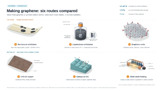
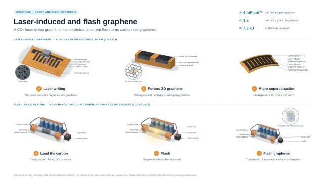
Six processing steps for graphene devices: annealing away PMMA residue, surface and substitutional chemical doping, ALD oxide on pristine and PTCA-functionalised graphene, ionic-liquid gating, one-dimensional edge contacts to hBN-encapsulated graphene, and the block-copolymer nanomesh.
Updated 11 cited papers45 editable layers

At a glance
- Category
- Graphene research
- Method
- Device processing
- Starting materials
- Transferred CVD or exfoliated graphene, hBN flakes
- Product
- Clean, doped, gated, contacted and patterned graphene devices
- Key result
- Stacks, molecules and masks drawn in 3D after the cited papers; residue amounts, molecule counts and layer heights are settings, drawn not to scale; the ionic double layer is schematic
- Figure
- 1920 × 1080 px (16:9), 45 editable layers, 6 generated objects
Step by step
- Clean: annealPMMA physisorbed on graphene decomposes in two steps of weight loss on annealing and cannot be removed entirely at a temperature graphene survives (Lin et al. 2012); residue stays on graphene but almost disappears from hBN and MoS₂ (Park et al. 2015); hBN/graphene/hBN stacks are annealed at 350 °C in ultra-high vacuum for 1 h (Xu et al. 2018)
- DopeAtoms swapped into the lattice (substitutional doping) or molecules on the surface that exchange charge with it (surface charge transfer); stable p-type doping is well established, n-type harder because most donors are unstable (Liu, Wei & Hu 2025); NO₂ is a strong acceptor (Wehling et al. 2008)
- Gate: ALD oxideOn pristine graphene ALD oxide grows only on edges and defect sites; after perylene tetracarboxylic acid (PTCA) functionalisation the coating is uniform and ultrathin, a route to thin high-κ gate dielectrics (Wang, Tabakman & Dai 2008)
- Gate: ionic liquidElectric double-layer transistors tune the carrier density of graphene continuously to beyond 10¹⁴ cm⁻² (Ye et al. 2011); the Fermi-level shift is set by the quantum capacitance in series with the double layer (George et al. 2018); the ions’ Coulomb scattering limits the mobility (Petach et al. 2017)
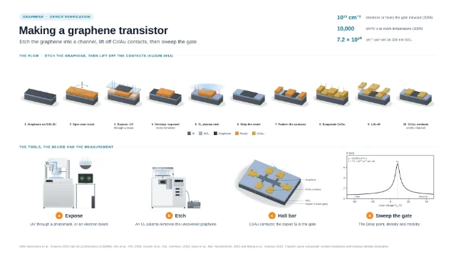
- Edge contactsOnly the one-dimensional edge of the graphene is metallised, which outperforms surface contacts (Wang et al. 2013); steps as Xu et al. (2018) give them: a PC/PDMS stamp picks up the top hBN and the graphene, lands them on the bottom hBN, the stack is annealed, etched and contacted with Cr/Au
- NanomeshBlock-copolymer lithography with P(S-b-MMA): periodicities of about 39 and 27 nm and necks down to about 5 nm; on–off ratio more than 100 at necks of ≈ 7 nm (Bai et al. 2010)
Strengths
- Edge contacts keep the channel encapsulated (Wang et al. 2013)
- Ionic gates reach densities solid gates cannot (Ye et al. 2011)
- The nanomesh opens a transport gap at the wafer scale (Bai et al. 2010)
Limitations
- PMMA cannot be annealed away entirely (Lin et al. 2012)
- n-type dopants are often unstable (Liu, Wei & Hu 2025)
- Ionic liquids limit the mobility (Petach et al. 2017)
Uses
- High-mobility devices
- Transparent and flexible transistors
- Semiconducting graphene films
Papers this template follows
- Lin et al., “Graphene annealing: how clean can it be?”, Nano Lett. 2012. doi:10.1021/nl203733rprimary
- Liu, Wei & Hu, “A review on n-type chemical doping of graphene films: preparation, characterization and applications”, Nanoscale 2025. doi:10.1039/d5nr02633dprimary
- Wang, Tabakman & Dai, “Atomic layer deposition of metal oxides on pristine and functionalized graphene”, J. Am. Chem. Soc. 2008. doi:10.1021/ja8023059primary
- Ye et al., “Accessing the transport properties of graphene and its multilayers at high carrier density”, PNAS 2011. doi:10.1073/pnas.1018388108primary
- Wang et al., “One-dimensional electrical contact to a two-dimensional material”, Science 2013. doi:10.1126/science.1244358primary
- Bai et al., “Graphene nanomesh”, Nat. Nanotechnol. 2010. doi:10.1038/nnano.2010.8primary
- Park et al., “Effective characterization of polymer residues on two-dimensional materials by Raman spectroscopy”, Nanotechnology 2015. doi:10.1088/0957-4484/26/48/485701further reading
- Xu et al., “Spin inversion in graphene spin valves by gate-tunable magnetic proximity effect at one-dimensional contacts”, Nat. Commun. 2018. doi:10.1038/s41467-018-05358-3further reading
- Wehling et al., “Molecular doping of graphene”, Nano Lett. 2008. doi:10.1021/nl072364wfurther reading
- George et al., “Probing the electric double-layer capacitance in a Keggin-type polyoxometalate ionic liquid gated graphene transistor”, Phys. Chem. Chem. Phys. 2018. doi:10.1039/c8cp02307gfurther reading
- Petach et al., “Disorder from the bulk ionic liquid in electric double layer transistors”, ACS Nano 2017. doi:10.1021/acsnano.7b03864further reading
Drawn by LabCanvas after Lin et al., Nano Lett. 2012 (doi:10.1021/nl203733r), Liu, Wei & Hu, Nanoscale 2025, Wang, Tabakman & Dai, JACS 2008, Ye et al., PNAS 2011, Wang et al., Science 2013, Xu et al., Nat. Commun. 2018, Bai et al., Nat. Nanotechnol. 2010, and the papers in the details.
How templates are written and checked: editorial guidelines.
Questions
What does the “Processing graphene devices” template show?
Six processing steps for graphene devices: annealing away PMMA residue, surface and substitutional chemical doping, ALD oxide on pristine and PTCA-functionalised graphene, ionic-liquid gating, one-dimensional edge contacts to hBN-encapsulated graphene, and the block-copolymer nanomesh.
What are the steps shown in “Processing graphene devices”?
1. Clean: anneal: PMMA physisorbed on graphene decomposes in two steps of weight loss on annealing and cannot be removed entirely at a temperature graphene survives (Lin et al. 2012); residue stays on graphene but almost disappears from hBN and MoS₂ (Park et al. 2015); hBN/graphene/hBN stacks are annealed at 350 °C in ultra-high vacuum for 1 h (Xu et al. 2018). 2. Dope: Atoms swapped into the lattice (substitutional doping) or molecules on the surface that exchange charge with it (surface charge transfer); stable p-type doping is well established, n-type harder because most donors are unstable (Liu, Wei & Hu 2025); NO₂ is a strong acceptor (Wehling et al. 2008). 3. Gate: ALD oxide: On pristine graphene ALD oxide grows only on edges and defect sites; after perylene tetracarboxylic acid (PTCA) functionalisation the coating is uniform and ultrathin, a route to thin high-κ gate dielectrics (Wang, Tabakman & Dai 2008). 4. Gate: ionic liquid: Electric double-layer transistors tune the carrier density of graphene continuously to beyond 10¹⁴ cm⁻² (Ye et al. 2011); the Fermi-level shift is set by the quantum capacitance in series with the double layer (George et al. 2018); the ions’ Coulomb scattering limits the mobility (Petach et al. 2017). 5. Edge contacts: Only the one-dimensional edge of the graphene is metallised, which outperforms surface contacts (Wang et al. 2013); steps as Xu et al. (2018) give them: a PC/PDMS stamp picks up the top hBN and the graphene, lands them on the bottom hBN, the stack is annealed, etched and contacted with Cr/Au. 6. Nanomesh: Block-copolymer lithography with P(S-b-MMA): periodicities of about 39 and 27 nm and necks down to about 5 nm; on–off ratio more than 100 at necks of ≈ 7 nm (Bai et al. 2010).
What are the starting materials and the product?
Starting materials: Transferred CVD or exfoliated graphene, hBN flakes. Product: Clean, doped, gated, contacted and patterned graphene devices.
Which papers is “Processing graphene devices” based on?
Lin et al., “Graphene annealing: how clean can it be?”, Nano Lett. 2012 (doi:10.1021/nl203733r); Liu, Wei & Hu, “A review on n-type chemical doping of graphene films: preparation, characterization and applications”, Nanoscale 2025 (doi:10.1039/d5nr02633d); Wang, Tabakman & Dai, “Atomic layer deposition of metal oxides on pristine and functionalized graphene”, J. Am. Chem. Soc. 2008 (doi:10.1021/ja8023059); Ye et al., “Accessing the transport properties of graphene and its multilayers at high carrier density”, PNAS 2011 (doi:10.1073/pnas.1018388108); Wang et al., “One-dimensional electrical contact to a two-dimensional material”, Science 2013 (doi:10.1126/science.1244358); Bai et al., “Graphene nanomesh”, Nat. Nanotechnol. 2010 (doi:10.1038/nnano.2010.8); Park et al., “Effective characterization of polymer residues on two-dimensional materials by Raman spectroscopy”, Nanotechnology 2015 (doi:10.1088/0957-4484/26/48/485701); Xu et al., “Spin inversion in graphene spin valves by gate-tunable magnetic proximity effect at one-dimensional contacts”, Nat. Commun. 2018 (doi:10.1038/s41467-018-05358-3); Wehling et al., “Molecular doping of graphene”, Nano Lett. 2008 (doi:10.1021/nl072364w); George et al., “Probing the electric double-layer capacitance in a Keggin-type polyoxometalate ionic liquid gated graphene transistor”, Phys. Chem. Chem. Phys. 2018 (doi:10.1039/c8cp02307g); Petach et al., “Disorder from the bulk ionic liquid in electric double layer transistors”, ACS Nano 2017 (doi:10.1021/acsnano.7b03864).
Can I edit the “Processing graphene devices” template?
Yes. Open it in the LabCanvas editor: all 45 layers are editable, including 6 generated objects (structures, plots, equipment) with their own settings. Change the text, colours and layout, then export PNG, TIFF, SVG or PDF.
Do I need an account to use this template?
Not to view it here. To open and edit it, sign in to LabCanvas or create a free account (the free plan keeps up to 3 designs). Downloading the figure is part of LabCanvas Pro (US$19 a month or US$199 a year).