Graphical abstract template · Graphene research · Microscopy guide
Seeing graphene: a microscopy guide
Six ways to look at graphene in one figure: optical contrast on SiO₂/Si, AFM heights and bubbles on hBN, SEM of CVD domains on copper, the TEM lattice and its diffraction, the STM moiré of graphene on hBN and LEED of epitaxial graphene on SiC.
Updated 10 cited papers46 editable layers

At a glance
- Category
- Graphene research
- Method
- Microscopy guide
- Starting materials
- Exfoliated graphene on SiO₂/Si and hBN, CVD graphene on Cu, graphene on SiC(0001)
- Product
- Where the flake is, how thick, its domains, its lattice and its stacking
- Key result
- Images computed by LabCanvas from optics, geometry and the reported structures; noise, field of view and spot brightness are settings
- Figure
- 1920 × 1080 px (16:9), 46 editable layers, 7 generated objects
Step by step
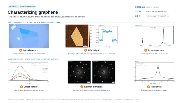
- Optical contrastColours computed from thin-film interference with n = 2.6 − 1.3i and 0.34 nm per layer; on oxidised silicon a single layer becomes visible (Blake et al. 2007)
- AFMEach layer adds graphite’s interlayer spacing, 0.335 nm; tapping mode can add up to about 1 nm (Nemes-Incze et al. 2008); round bubbles of trapped contamination keep an aspect ratio h/R ≈ 0.11 (Khestanova et al. 2016)
- SEMHexagonal domains on commercial Cu foil turned every which way and nucleating in rows (Robertson & Warner 2011; Yang et al. 2012); regions with more layers are darker (Liu et al. 2021; Kondrashov et al. 2021)
- TEMLattice images of the honeycomb, and electron diffraction with spots at d = a√3/2 and a/2 for a = 2.46 Å, the periodicities of 2.13 and 1.23 Å (Meyer et al. 2007)
- STMThe moiré of graphene on hBN, whose wavelength follows the twist and hBN’s 1.8 % larger lattice (Yankowitz et al. 2012)
- LEEDOn SiC(0001): SiC (1 × 1) spots, graphene (1 × 1) spots turned 30° from them and the (6√3 × 6√3)R30° spots of the coincidence cell (Riedl et al. 2009)
Strengths
- Optical contrast finds flakes in seconds (Blake et al. 2007)
- AFM and TEM count layers directly
- STM and LEED show stacking and orientation
Limitations
- AFM heights of thin flakes can be off by about 1 nm (Nemes-Incze et al. 2008)
- TEM diffraction needs suspended sheets (Meyer et al. 2007)
- LEED needs a crystalline substrate and ultra-high vacuum
Uses
- Choosing flakes for devices
- Inspecting CVD growth
- Checking twist and alignment in stacks
Papers this template follows
- Blake et al., “Making graphene visible”, Appl. Phys. Lett. 2007. doi:10.1063/1.2768624primary
- Nemes-Incze et al., “Anomalies in thickness measurements of graphene and few layer graphite crystals by tapping mode atomic force microscopy”, Carbon 2008. doi:10.1016/j.carbon.2008.06.022primary
- Meyer et al., “The structure of suspended graphene sheets”, Nature 2007. doi:10.1038/nature05545primary
- Yankowitz et al., “Emergence of superlattice Dirac points in graphene on hexagonal boron nitride”, Nat. Phys. 2012. doi:10.1038/nphys2272primary
- Riedl et al., “Quasi-free-standing epitaxial graphene on SiC obtained by hydrogen intercalation”, Phys. Rev. Lett. 2009. doi:10.1103/PhysRevLett.103.246804primary
- Khestanova et al., “Universal shape and pressure inside bubbles appearing in van der Waals heterostructures”, Nat. Commun. 2016. doi:10.1038/ncomms12587further reading
- Robertson & Warner, “Hexagonal single crystal domains of few-layer graphene on copper foils”, Nano Lett. 2011. doi:10.1021/nl104142kfurther reading
- Yang et al., “A facile method to observe graphene growth on copper foil”, Nanotechnology 2012. doi:10.1088/0957-4484/23/47/475705further reading
- Liu et al., “Sequential growth and twisted stacking of chemical-vapor-deposited graphene”, Nanoscale Adv. 2021. doi:10.1039/d0na00982bfurther reading
- Kondrashov et al., “Preparation of copper surface for the synthesis of single-layer graphene”, Nanomaterials 2021. doi:10.3390/nano11051071further reading
Computed by LabCanvas after Blake et al., APL 2007, Nemes-Incze et al., Carbon 2008, Khestanova et al., Nat. Commun. 2016, Meyer et al., Nature 2007, Yankowitz et al., Nat. Phys. 2012, Riedl et al., PRL 2009, and the papers in the details.
How templates are written and checked: editorial guidelines.
Questions
What does the “Seeing graphene: a microscopy guide” template show?
Six ways to look at graphene in one figure: optical contrast on SiO₂/Si, AFM heights and bubbles on hBN, SEM of CVD domains on copper, the TEM lattice and its diffraction, the STM moiré of graphene on hBN and LEED of epitaxial graphene on SiC.
What are the steps shown in “Seeing graphene: a microscopy guide”?
1. Optical contrast: Colours computed from thin-film interference with n = 2.6 − 1.3i and 0.34 nm per layer; on oxidised silicon a single layer becomes visible (Blake et al. 2007). 2. AFM: Each layer adds graphite’s interlayer spacing, 0.335 nm; tapping mode can add up to about 1 nm (Nemes-Incze et al. 2008); round bubbles of trapped contamination keep an aspect ratio h/R ≈ 0.11 (Khestanova et al. 2016). 3. SEM: Hexagonal domains on commercial Cu foil turned every which way and nucleating in rows (Robertson & Warner 2011; Yang et al. 2012); regions with more layers are darker (Liu et al. 2021; Kondrashov et al. 2021). 4. TEM: Lattice images of the honeycomb, and electron diffraction with spots at d = a√3/2 and a/2 for a = 2.46 Å, the periodicities of 2.13 and 1.23 Å (Meyer et al. 2007). 5. STM: The moiré of graphene on hBN, whose wavelength follows the twist and hBN’s 1.8 % larger lattice (Yankowitz et al. 2012). 6. LEED: On SiC(0001): SiC (1 × 1) spots, graphene (1 × 1) spots turned 30° from them and the (6√3 × 6√3)R30° spots of the coincidence cell (Riedl et al. 2009).
What are the starting materials and the product?
Starting materials: Exfoliated graphene on SiO₂/Si and hBN, CVD graphene on Cu, graphene on SiC(0001). Product: Where the flake is, how thick, its domains, its lattice and its stacking.
Which papers is “Seeing graphene: a microscopy guide” based on?
Blake et al., “Making graphene visible”, Appl. Phys. Lett. 2007 (doi:10.1063/1.2768624); Nemes-Incze et al., “Anomalies in thickness measurements of graphene and few layer graphite crystals by tapping mode atomic force microscopy”, Carbon 2008 (doi:10.1016/j.carbon.2008.06.022); Meyer et al., “The structure of suspended graphene sheets”, Nature 2007 (doi:10.1038/nature05545); Yankowitz et al., “Emergence of superlattice Dirac points in graphene on hexagonal boron nitride”, Nat. Phys. 2012 (doi:10.1038/nphys2272); Riedl et al., “Quasi-free-standing epitaxial graphene on SiC obtained by hydrogen intercalation”, Phys. Rev. Lett. 2009 (doi:10.1103/PhysRevLett.103.246804); Khestanova et al., “Universal shape and pressure inside bubbles appearing in van der Waals heterostructures”, Nat. Commun. 2016 (doi:10.1038/ncomms12587); Robertson & Warner, “Hexagonal single crystal domains of few-layer graphene on copper foils”, Nano Lett. 2011 (doi:10.1021/nl104142k); Yang et al., “A facile method to observe graphene growth on copper foil”, Nanotechnology 2012 (doi:10.1088/0957-4484/23/47/475705); Liu et al., “Sequential growth and twisted stacking of chemical-vapor-deposited graphene”, Nanoscale Adv. 2021 (doi:10.1039/d0na00982b); Kondrashov et al., “Preparation of copper surface for the synthesis of single-layer graphene”, Nanomaterials 2021 (doi:10.3390/nano11051071).
Can I edit the “Seeing graphene: a microscopy guide” template?
Yes. Open it in the LabCanvas editor: all 46 layers are editable, including 7 generated objects (structures, plots, equipment) with their own settings. Change the text, colours and layout, then export PNG, TIFF, SVG or PDF.
Do I need an account to use this template?
Not to view it here. To open and edit it, sign in to LabCanvas or create a free account (the free plan keeps up to 3 designs). Downloading the figure is part of LabCanvas Pro (US$19 a month or US$199 a year).