Graphical abstract template · Graphene synthesis · Chemical vapour deposition · Bottom-up
CVD graphene on copper and PMMA transfer
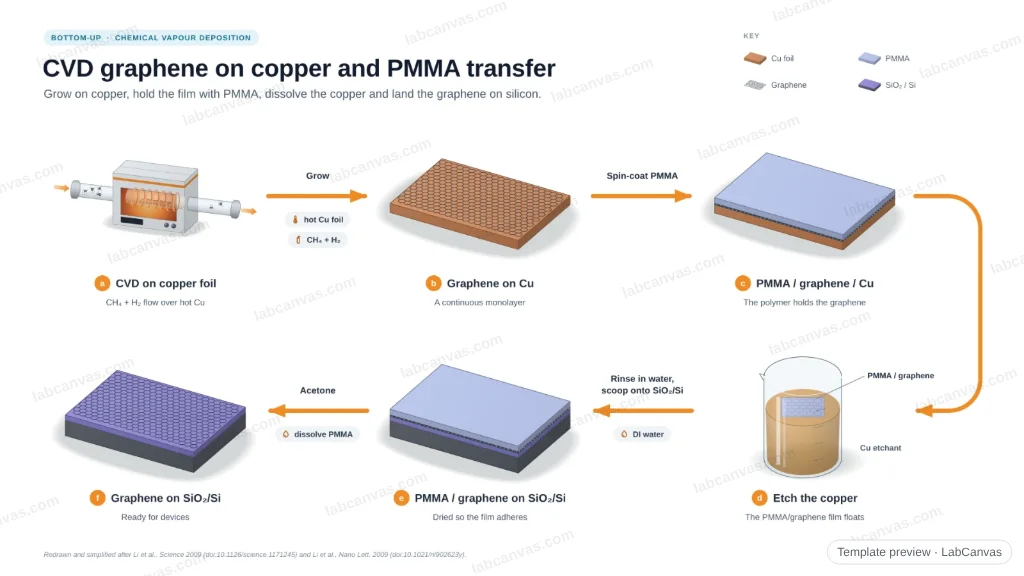
Graphene grown by CVD on copper foil has to be moved onto an insulating substrate before it can be used in devices. A thin PMMA film is spin-coated on top as a support, the copper is etched away so that the PMMA/graphene film floats, and the film is scooped onto SiO₂/Si; acetone then dissolves the PMMA.
Updated 4 cited papers68 editable layers
At a glance
- Category
- Graphene synthesis
- Method
- Chemical vapour deposition
- Approach
- Bottom-up
- Starting materials
- Copper foil; CH₄ and H₂
- Product
- Monolayer graphene on SiO₂/Si (or another target substrate)
- Typical size
- Centimetre-scale films, limited by the foil and the furnace
- Key result
- High: mostly monolayer, electron mobility up to 4050 cm²/V·s reported; transfer adds wrinkles, cracks and residue
- Scalability
- High for growth; the transfer is the bottleneck
- Figure
- 1920 × 1080 px (16:9), 68 editable layers, 14 generated objects
Step by step
- CVD growthCH₄ (with H₂) over hot Cu foil in a tube furnace
- Spin-coat PMMAA thin polymer film supports the graphene
- Etch the copperFloat the stack on a copper etchant (for example aqueous FeCl₃) until the copper is gone
- Rinse and scoopRinse the floating film in water and lift it onto SiO₂/Si
- Remove the PMMADissolve the polymer in acetone
Strengths
- Large-area monolayer films
- Works with almost any target substrate
- Simple, widely used lab procedure
Limitations
- PMMA residue and etchant ions contaminate the graphene
- Tears and wrinkles from handling
- The copper foil is used up
Uses
- Transparent conductive electrodes
- Field-effect transistors and sensors
- Membranes and coatings
Papers this template follows
- Li et al., “Large-area synthesis of high-quality and uniform graphene films on copper foils”, Science 2009. doi:10.1126/science.1171245primary
- Li et al., “Transfer of large-area graphene films for high-performance transparent conductive electrodes”, Nano Lett. 2009. doi:10.1021/nl902623yprimary
- Sun et al., “Synthesis of wafer-scale graphene with chemical vapor deposition for electronic device applications”, Adv. Mater. Technol. 2021. doi:10.1002/admt.202000744review
- Bonaccorso et al., “Production and processing of graphene and 2d crystals”, Mater. Today 2012. doi:10.1016/S1369-7021(13)70014-2review
Redrawn and simplified after Li et al., Science 2009 (doi:10.1126/science.1171245) and Li et al., Nano Lett. 2009 (doi:10.1021/nl902623y).
How templates are written and checked: editorial guidelines.
Questions
What does the “CVD graphene on copper and PMMA transfer” template show?
Graphene grown by CVD on copper foil has to be moved onto an insulating substrate before it can be used in devices. A thin PMMA film is spin-coated on top as a support, the copper is etched away so that the PMMA/graphene film floats, and the film is scooped onto SiO₂/Si; acetone then dissolves the PMMA.
What are the steps shown in “CVD graphene on copper and PMMA transfer”?
1. CVD growth: CH₄ (with H₂) over hot Cu foil in a tube furnace. 2. Spin-coat PMMA: A thin polymer film supports the graphene. 3. Etch the copper: Float the stack on a copper etchant (for example aqueous FeCl₃) until the copper is gone. 4. Rinse and scoop: Rinse the floating film in water and lift it onto SiO₂/Si. 5. Remove the PMMA: Dissolve the polymer in acetone.
What are the starting materials and the product?
Starting materials: Copper foil; CH₄ and H₂. Product: Monolayer graphene on SiO₂/Si (or another target substrate).
Which papers is “CVD graphene on copper and PMMA transfer” based on?
Li et al., “Large-area synthesis of high-quality and uniform graphene films on copper foils”, Science 2009 (doi:10.1126/science.1171245); Li et al., “Transfer of large-area graphene films for high-performance transparent conductive electrodes”, Nano Lett. 2009 (doi:10.1021/nl902623y); Sun et al., “Synthesis of wafer-scale graphene with chemical vapor deposition for electronic device applications”, Adv. Mater. Technol. 2021 (doi:10.1002/admt.202000744); Bonaccorso et al., “Production and processing of graphene and 2d crystals”, Mater. Today 2012 (doi:10.1016/S1369-7021(13)70014-2).
Can I edit the “CVD graphene on copper and PMMA transfer” template?
Yes. Open it in the LabCanvas editor: all 68 layers are editable, including 14 generated objects (structures, plots, equipment) with their own settings. Change the text, colours and layout, then export PNG, TIFF, SVG or PDF.
Do I need an account to use this template?
Not to view it here. To open and edit it, sign in to LabCanvas or create a free account (the free plan keeps one design of each kind). Downloading the figure is part of LabCanvas Pro (US$19 a month or US$199 a year).