Graphical abstract template · Graphene synthesis · Epitaxial growth on SiC · Bottom-up
Graphene on SiC for remote epitaxy and layer transfer
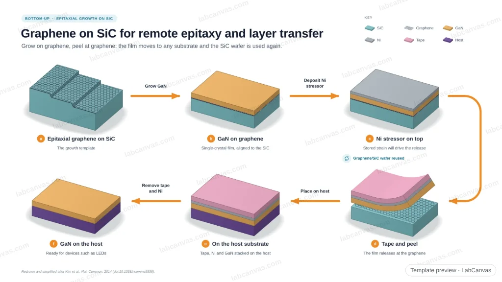
Epitaxial graphene on SiC can serve as a reusable growth template. A single-crystal GaN film is grown on the graphene, a nickel stressor layer and tape are added, and the film peels off cleanly along the weak graphene interface. It is then placed on any host substrate, while the graphene/SiC wafer goes back for the next growth.
Updated 3 cited papers59 editable layers
At a glance
- Category
- Graphene synthesis
- Method
- Epitaxial growth on SiC
- Approach
- Bottom-up
- Starting materials
- Epitaxial graphene on a SiC wafer
- Product
- A single-crystal GaN film on a host substrate of choice, and a reusable graphene/SiC wafer
- Typical size
- Wafer-scale films
- Key result
- Single-crystal GaN with about 4 × 10⁸ cm⁻² defects, released with a smooth surface
- Scalability
- Medium: wafer-scale, and the costly substrate is reused
- Figure
- 1920 × 1080 px (16:9), 59 editable layers, 13 generated objects
Step by step
- Epitaxial graphene on SiCGraphene grown on the SiC wafer is the growth template
- Grow GaNSingle-crystal GaN grows on the graphene, aligned by the substrate
- Deposit a Ni stressorA strained nickel film on top drives the release
- Tape and peelWith tape on the Ni, the GaN/Ni film releases at the weak graphene interface
- Place on a hostStick the film onto the target substrate
- Remove tape and NiGaN stays on the host; the graphene/SiC wafer is reused
Strengths
- The expensive SiC wafer can be reused
- Clean, precise release at the graphene interface
- Films move onto flexible or foreign substrates
Limitations
- Needs high-quality epitaxial graphene
- The graphene interface limits film quality
- Extra stressor and tape steps
Uses
- Transferable and flexible LEDs
- Heterogeneous integration of semiconductors
- Freestanding single-crystal membranes
Papers this template follows
- Kim et al., “Principle of direct van der Waals epitaxy of single-crystalline films on epitaxial graphene”, Nat. Commun. 2014. doi:10.1038/ncomms5836primary
- Kim et al., “Remote epitaxy through graphene enables two-dimensional material-based layer transfer”, Nature 2017. doi:10.1038/nature22053further reading
- Emtsev et al., “Towards wafer-size graphene layers by atmospheric pressure graphitization of silicon carbide”, Nat. Mater. 2009. doi:10.1038/nmat2382further reading
Redrawn and simplified after Kim et al., Nat. Commun. 2014 (doi:10.1038/ncomms5836).
How templates are written and checked: editorial guidelines.
Questions
What does the “Graphene on SiC for remote epitaxy and layer transfer” template show?
Epitaxial graphene on SiC can serve as a reusable growth template. A single-crystal GaN film is grown on the graphene, a nickel stressor layer and tape are added, and the film peels off cleanly along the weak graphene interface. It is then placed on any host substrate, while the graphene/SiC wafer goes back for the next growth.
What are the steps shown in “Graphene on SiC for remote epitaxy and layer transfer”?
1. Epitaxial graphene on SiC: Graphene grown on the SiC wafer is the growth template. 2. Grow GaN: Single-crystal GaN grows on the graphene, aligned by the substrate. 3. Deposit a Ni stressor: A strained nickel film on top drives the release. 4. Tape and peel: With tape on the Ni, the GaN/Ni film releases at the weak graphene interface. 5. Place on a host: Stick the film onto the target substrate. 6. Remove tape and Ni: GaN stays on the host; the graphene/SiC wafer is reused.
What are the starting materials and the product?
Starting materials: Epitaxial graphene on a SiC wafer. Product: A single-crystal GaN film on a host substrate of choice, and a reusable graphene/SiC wafer.
Which papers is “Graphene on SiC for remote epitaxy and layer transfer” based on?
Kim et al., “Principle of direct van der Waals epitaxy of single-crystalline films on epitaxial graphene”, Nat. Commun. 2014 (doi:10.1038/ncomms5836); Kim et al., “Remote epitaxy through graphene enables two-dimensional material-based layer transfer”, Nature 2017 (doi:10.1038/nature22053); Emtsev et al., “Towards wafer-size graphene layers by atmospheric pressure graphitization of silicon carbide”, Nat. Mater. 2009 (doi:10.1038/nmat2382).
Can I edit the “Graphene on SiC for remote epitaxy and layer transfer” template?
Yes. Open it in the LabCanvas editor: all 59 layers are editable, including 13 generated objects (structures, plots, equipment) with their own settings. Change the text, colours and layout, then export PNG, TIFF, SVG or PDF.
Do I need an account to use this template?
Not to view it here. To open and edit it, sign in to LabCanvas or create a free account (the free plan keeps one design of each kind). Downloading the figure is part of LabCanvas Pro (US$19 a month or US$199 a year).