Graphical abstract template · Graphical abstracts · Graphical abstract
Ferroelectric hafnium oxide: a polar phase in a chip dielectric
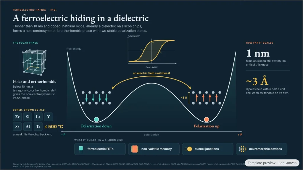
An energy landscape for ferroelectric HfO₂: a double well whose two minima are the two polarization states and whose barrier an electric field pushes the film over. Around it: how thin, doped hafnia forms a non-centrosymmetric orthorhombic phase (live 3D cell), why it suits silicon processing, how far it scales (switching at 1 nm, dipoles ~3 Å wide) and the memories it enables.
Updated 6 cited papers91 editable layers
At a glance
- Category
- Graphical abstracts
- Method
- Graphical abstract
- Starting materials
- Hafnium oxide, a fluorite-structure dielectric already used on silicon chips
- Product
- Doped HfO₂ films under 10 nm with a switchable spontaneous polarization
- Key result
- Polarization switchable down to 1 nm (Cheema et al. 2020); dipoles ~3 Å wide (Lee et al. 2020); ALD anneal ≤ 500 °C (Huang et al. 2025)
- Figure
- 1920 × 1080 px (16:9), 91 editable layers, 5 generated objects
Step by step
- A polar phaseIn sub-10 nm films a tetragonal-to-orthorhombic transition yields the non-centrosymmetric Pbc2₁ phase, hence a spontaneous polarization (Müller et al. 2012); the phase is metastable and stabilized by doping (Yan et al. 2024)
- Doped and grown on siliconDopants such as Zr, Si, La, Y, Sr, Al and Ta; atomic layer deposition with annealing at ≤ 500 °C fits the CMOS back end of line (Huang et al. 2025)
- Two wellsTwo stable polarization states, switched by an electric field (Cheema et al. 2020; schematic double well)
- Scale-freeSwitchable polarization down to 1 nm on silicon, with no critical thickness (Cheema et al. 2020); dipoles localized within ~3 Å half-unit cells, individually switchable (Lee et al. 2020)
- DevicesFerroelectric memristors, tunnel junctions and field-effect transistors, including for neuromorphic computing (Jayakrishnan et al. 2024)
Uses
- Graphical abstracts on HfO₂-based ferroelectrics
- Talks on ferroelectric memories and CMOS-compatible ferroelectrics
- Teaching double-well polarization switching
Papers this template follows
- Müller et al., “Ferroelectricity in simple binary ZrO2 and HfO2”, Nano Lett. 2012. doi:10.1021/nl302049kprimary
- Cheema et al., “Enhanced ferroelectricity in ultrathin films grown directly on silicon”, Nature 2020. doi:10.1038/s41586-020-2208-xprimary
- Lee et al., “Scale-free ferroelectricity induced by flat phonon bands in HfO2”, Science 2020. doi:10.1126/science.aba0067primary
- Huang et al., “Structure, properties and applications of HfO2-based piezoelectric films”, Nanoscale 2025. doi:10.1039/d5nr02530creview
- Yan et al., “Recent progress on defect-engineering in ferroelectric HfO2: the next step forward via multiscale structural optimization”, Mater. Horiz. 2024. doi:10.1039/d3mh01273ereview
- Jayakrishnan et al., “Growth of emergent simple pseudo-binary ferroelectrics and their potential in neuromorphic computing devices”, Mater. Horiz. 2024. doi:10.1039/d4mh00153breview
Drawn by LabCanvas after Müller et al., Nano Lett. 2012 (doi:10.1021/nl302049k); Cheema et al., Nature 2020 (doi:10.1038/s41586-020-2208-x); Lee et al., Science 2020 (doi:10.1126/science.aba0067); Huang et al., Nanoscale 2025 (doi:10.1039/d5nr02530c); Jayakrishnan et al., Mater. Horiz. 2024 (doi:10.1039/d4mh00153b).
How templates are written and checked: editorial guidelines.
Questions
What does the “Ferroelectric hafnium oxide: a polar phase in a chip dielectric” template show?
An energy landscape for ferroelectric HfO₂: a double well whose two minima are the two polarization states and whose barrier an electric field pushes the film over. Around it: how thin, doped hafnia forms a non-centrosymmetric orthorhombic phase (live 3D cell), why it suits silicon processing, how far it scales (switching at 1 nm, dipoles ~3 Å wide) and the memories it enables.
What are the steps shown in “Ferroelectric hafnium oxide: a polar phase in a chip dielectric”?
1. A polar phase: In sub-10 nm films a tetragonal-to-orthorhombic transition yields the non-centrosymmetric Pbc2₁ phase, hence a spontaneous polarization (Müller et al. 2012); the phase is metastable and stabilized by doping (Yan et al. 2024). 2. Doped and grown on silicon: Dopants such as Zr, Si, La, Y, Sr, Al and Ta; atomic layer deposition with annealing at ≤ 500 °C fits the CMOS back end of line (Huang et al. 2025). 3. Two wells: Two stable polarization states, switched by an electric field (Cheema et al. 2020; schematic double well). 4. Scale-free: Switchable polarization down to 1 nm on silicon, with no critical thickness (Cheema et al. 2020); dipoles localized within ~3 Å half-unit cells, individually switchable (Lee et al. 2020). 5. Devices: Ferroelectric memristors, tunnel junctions and field-effect transistors, including for neuromorphic computing (Jayakrishnan et al. 2024).
What are the starting materials and the product?
Starting materials: Hafnium oxide, a fluorite-structure dielectric already used on silicon chips. Product: Doped HfO₂ films under 10 nm with a switchable spontaneous polarization.
Which papers is “Ferroelectric hafnium oxide: a polar phase in a chip dielectric” based on?
Müller et al., “Ferroelectricity in simple binary ZrO2 and HfO2”, Nano Lett. 2012 (doi:10.1021/nl302049k); Cheema et al., “Enhanced ferroelectricity in ultrathin films grown directly on silicon”, Nature 2020 (doi:10.1038/s41586-020-2208-x); Lee et al., “Scale-free ferroelectricity induced by flat phonon bands in HfO2”, Science 2020 (doi:10.1126/science.aba0067); Huang et al., “Structure, properties and applications of HfO2-based piezoelectric films”, Nanoscale 2025 (doi:10.1039/d5nr02530c); Yan et al., “Recent progress on defect-engineering in ferroelectric HfO2: the next step forward via multiscale structural optimization”, Mater. Horiz. 2024 (doi:10.1039/d3mh01273e); Jayakrishnan et al., “Growth of emergent simple pseudo-binary ferroelectrics and their potential in neuromorphic computing devices”, Mater. Horiz. 2024 (doi:10.1039/d4mh00153b).
Can I edit the “Ferroelectric hafnium oxide: a polar phase in a chip dielectric” template?
Yes. Open it in the LabCanvas editor: all 91 layers are editable, including 5 generated objects (structures, plots, equipment) with their own settings. Change the text, colours and layout, then export PNG, TIFF, SVG or PDF.
Do I need an account to use this template?
Not to view it here. To open and edit it, sign in to LabCanvas or create a free account (the free plan keeps up to 3 designs). Downloading the figure is part of LabCanvas Pro (US$19 a month or US$199 a year).