Graphical abstract template · Materials graphical abstracts · Graphical abstract
Perovskite solar cell: from crystal to device
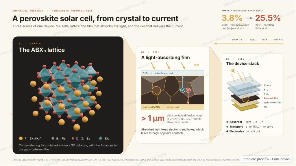
A zoom-in cascade through a perovskite solar cell: the device stack, its light-absorbing polycrystalline film between the two charge contacts, and the ABX₃ crystal of corner-sharing octahedra as a live 3D model. Light frees electrons and holes in the film; TiO₂ takes the electrons, spiro-OMeTAD the holes, and the electrodes carry the current out. Milestones from 3.8% in 2009 to a certified 25.5% in 2021.
Updated 7 cited papers81 editable layers
At a glance
- Category
- Materials graphical abstracts
- Method
- Graphical abstract
- Starting materials
- Methylammonium iodide and PbI₂, which react to (CH₃NH₃)PbI₃ (Kim et al. 2012)
- Product
- A perovskite cell: FTO glass / TiO₂ / perovskite / spiro-OMeTAD / Au
- Key result
- 3.8% for the first CH₃NH₃PbI₃-sensitised cell (Kojima et al. 2009); 9.7% all-solid-state with spiro-MeOTAD (Kim et al. 2012); diffusion lengths > 1 µm in CH₃NH₃PbI₃₋ₓClₓ vs ~100 nm in CH₃NH₃PbI₃ (Stranks et al. 2013); 25.8%, certified 25.5% (Min et al. 2021)
- Figure
- 1920 × 1080 px (16:9), 81 editable layers, 3 generated objects
Step by step
- The crystalABX₃: a 3D network of corner-sharing BX₆ octahedra (B = Pb, X = I or Br) with methylammonium (A) between them
- The filmA polycrystalline perovskite layer absorbs the light; in mixed-halide CH₃NH₃PbI₃₋ₓClₓ electrons and holes diffuse more than 1 µm
- The cellLayers on FTO glass: TiO₂ (electron contact), the perovskite absorber, spiro-OMeTAD (hole contact) and a gold electrode
- Light to currentHoles go into spiro-OMeTAD, electrons into TiO₂, and both are collected at the front and back contacts as photocurrent
Uses
- Graphical abstracts
- Talks and posters on perovskite photovoltaics
- Teaching how a thin-film solar cell works
Papers this template follows
- Kojima, Teshima, Shirai & Miyasaka, “Organometal halide perovskites as visible-light sensitizers for photovoltaic cells”, J. Am. Chem. Soc. 2009. doi:10.1021/ja809598rprimary
- Kim, Lee, Im, Lee, Moehl, Marchioro, Moon, Humphry-Baker, Yum, Moser, Grätzel & Park, “Lead iodide perovskite sensitized all-solid-state submicron thin film mesoscopic solar cell with efficiency exceeding 9%”, Sci. Rep. 2012. doi:10.1038/srep00591primary
- Stranks, Eperon, Grancini, Menelaou, Alcocer, Leijtens, Herz, Petrozza & Snaith, “Electron-hole diffusion lengths exceeding 1 micrometer in an organometal trihalide perovskite absorber”, Science 2013. doi:10.1126/science.1243982primary
- Min, Lee, Kim, Kim, Lee, Kim, Paik, Kim, Kim, Kim, Shin & Seok, “Perovskite solar cells with atomically coherent interlayers on SnO₂ electrodes”, Nature 2021. doi:10.1038/s41586-021-03964-8primary
- Jena, Kulkarni & Miyasaka, “Halide Perovskite Photovoltaics: Background, Status, and Future Prospects”, Chem. Rev. 2019. doi:10.1021/acs.chemrev.8b00539review
- Farigliano, Gomes-Filho, Reily Rocha & Martini Dalpian, “Precessional Dynamics of Octahedra in CsPbBr₃”, J. Chem. Theory Comput. 2026. doi:10.1021/acs.jctc.5c02166further reading
- Xie, Morgenstein, Hansen, … Blum & Mitzi, “Dimensionality-Controlled Confinement Effects for Tunable Optoelectronic Properties in Quasi-1D Hybrid Perovskites”, ACS Nano 2025. doi:10.1021/acsnano.4c16359further reading
Drawn by LabCanvas after Kojima et al., J. Am. Chem. Soc. 2009 (doi:10.1021/ja809598r), Kim et al., Sci. Rep. 2012 (doi:10.1038/srep00591), Stranks et al., Science 2013 (doi:10.1126/science.1243982) and Min et al., Nature 2021 (doi:10.1038/s41586-021-03964-8). Crystal, film and stack schematic.
How templates are written and checked: editorial guidelines.
Questions
What does the “Perovskite solar cell: from crystal to device” template show?
A zoom-in cascade through a perovskite solar cell: the device stack, its light-absorbing polycrystalline film between the two charge contacts, and the ABX₃ crystal of corner-sharing octahedra as a live 3D model. Light frees electrons and holes in the film; TiO₂ takes the electrons, spiro-OMeTAD the holes, and the electrodes carry the current out. Milestones from 3.8% in 2009 to a certified 25.5% in 2021.
What are the steps shown in “Perovskite solar cell: from crystal to device”?
1. The crystal: ABX₃: a 3D network of corner-sharing BX₆ octahedra (B = Pb, X = I or Br) with methylammonium (A) between them. 2. The film: A polycrystalline perovskite layer absorbs the light; in mixed-halide CH₃NH₃PbI₃₋ₓClₓ electrons and holes diffuse more than 1 µm. 3. The cell: Layers on FTO glass: TiO₂ (electron contact), the perovskite absorber, spiro-OMeTAD (hole contact) and a gold electrode. 4. Light to current: Holes go into spiro-OMeTAD, electrons into TiO₂, and both are collected at the front and back contacts as photocurrent.
What are the starting materials and the product?
Starting materials: Methylammonium iodide and PbI₂, which react to (CH₃NH₃)PbI₃ (Kim et al. 2012). Product: A perovskite cell: FTO glass / TiO₂ / perovskite / spiro-OMeTAD / Au.
Which papers is “Perovskite solar cell: from crystal to device” based on?
Kojima, Teshima, Shirai & Miyasaka, “Organometal halide perovskites as visible-light sensitizers for photovoltaic cells”, J. Am. Chem. Soc. 2009 (doi:10.1021/ja809598r); Kim, Lee, Im, Lee, Moehl, Marchioro, Moon, Humphry-Baker, Yum, Moser, Grätzel & Park, “Lead iodide perovskite sensitized all-solid-state submicron thin film mesoscopic solar cell with efficiency exceeding 9%”, Sci. Rep. 2012 (doi:10.1038/srep00591); Stranks, Eperon, Grancini, Menelaou, Alcocer, Leijtens, Herz, Petrozza & Snaith, “Electron-hole diffusion lengths exceeding 1 micrometer in an organometal trihalide perovskite absorber”, Science 2013 (doi:10.1126/science.1243982); Min, Lee, Kim, Kim, Lee, Kim, Paik, Kim, Kim, Kim, Shin & Seok, “Perovskite solar cells with atomically coherent interlayers on SnO₂ electrodes”, Nature 2021 (doi:10.1038/s41586-021-03964-8); Jena, Kulkarni & Miyasaka, “Halide Perovskite Photovoltaics: Background, Status, and Future Prospects”, Chem. Rev. 2019 (doi:10.1021/acs.chemrev.8b00539); Farigliano, Gomes-Filho, Reily Rocha & Martini Dalpian, “Precessional Dynamics of Octahedra in CsPbBr₃”, J. Chem. Theory Comput. 2026 (doi:10.1021/acs.jctc.5c02166); Xie, Morgenstein, Hansen, … Blum & Mitzi, “Dimensionality-Controlled Confinement Effects for Tunable Optoelectronic Properties in Quasi-1D Hybrid Perovskites”, ACS Nano 2025 (doi:10.1021/acsnano.4c16359).
Can I edit the “Perovskite solar cell: from crystal to device” template?
Yes. Open it in the LabCanvas editor: all 81 layers are editable, including 3 generated objects (structures, plots, equipment) with their own settings. Change the text, colours and layout, then export PNG, TIFF, SVG or PDF.
Do I need an account to use this template?
Not to view it here. To open and edit it, sign in to LabCanvas or create a free account (the free plan keeps up to 3 designs). Downloading the figure is part of LabCanvas Pro (US$19 a month or US$199 a year).