Graphical abstract template · Materials graphical abstracts · Graphical abstract
Monolayer MoS₂: from one atomic layer to logic
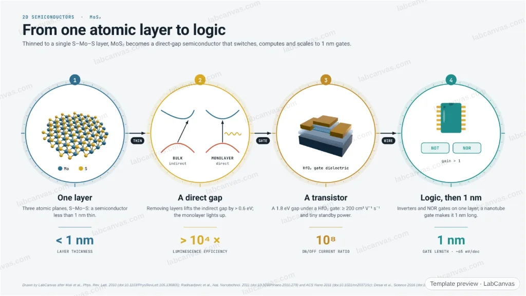
A chain of four lenses builds a chip up from one S–Mo–S layer: thinned to a monolayer, MoS₂ turns into a direct-gap semiconductor that lights up; a top-gated monolayer transistor switches by a factor of 10⁸; and the layer carries inverters, NOR logic and gates just 1 nm long.
Updated 6 cited papers218 editable layers
At a glance
- Category
- Materials graphical abstracts
- Method
- Graphical abstract
- Starting materials
- Layered MoS₂, an indirect-gap semiconductor in the bulk
- Product
- Single-layer MoS₂ transistors and logic circuits
- Key result
- On/off 1 × 10⁸ and ≥ 200 cm² V⁻¹ s⁻¹ (Radisavljevic et al. 2011); > 10⁴-fold luminescence efficiency (Mak et al. 2010); 1 nm gate, ~65 mV/dec (Desai et al. 2016)
- Figure
- 1920 × 1080 px (16:9), 218 editable layers, 1 generated objects
Step by step
- One layerThin MoS₂ down to a single S–Mo–S layer, less than 1 nm thin (Mak et al. 2010; Radisavljevic et al. 2011)
- Direct gapThe indirect gap rises by more than 0.6 eV as layers are removed, the monolayer becomes direct-gap and its luminescence efficiency rises more than 10⁴-fold (Mak et al. 2010; Splendiani et al. 2010)
- TransistorA 1.8 eV gap and a HfO₂ gate dielectric give mobility of at least 200 cm² V⁻¹ s⁻¹ and on/off ratios of 1 × 10⁸ (Radisavljevic et al. 2011)
- Logic and scalingInverters with gain above 1 and NOR gates on one layer (Radisavljevic et al. 2011, ACS Nano); a 1 nm gate with ~65 mV per decade, where silicon is predicted to fail below 5 nm (Desai et al. 2016)
Uses
- Graphical abstracts on 2D semiconductors and TMD electronics
- Talks on monolayer transistors and scaling beyond silicon
- Teaching indirect-to-direct band gap crossover
Papers this template follows
- Mak, Lee, Hone, Shan & Heinz, “Atomically thin MoS₂: a new direct-gap semiconductor”, Phys. Rev. Lett. 2010. doi:10.1103/PhysRevLett.105.136805primary
- Splendiani et al., “Emerging photoluminescence in monolayer MoS2”, Nano Lett. 2010. doi:10.1021/nl903868wprimary
- Radisavljevic, Radenovic, Brivio, Giacometti & Kis, “Single-layer MoS2 transistors”, Nat. Nanotechnol. 2011. doi:10.1038/nnano.2010.279method origin
- Radisavljevic, Whitwick & Kis, “Integrated circuits and logic operations based on single-layer MoS2”, ACS Nano 2011. doi:10.1021/nn203715cprimary
- Desai et al., “MoS2 transistors with 1-nanometer gate lengths”, Science 2016. doi:10.1126/science.aah4698primary
- Akinwande et al., “Graphene and two-dimensional materials for silicon technology”, Nature 2019. doi:10.1038/s41586-019-1573-9review
Drawn by LabCanvas after Mak et al., Phys. Rev. Lett. 2010 (doi:10.1103/PhysRevLett.105.136805); Radisavljevic et al., Nat. Nanotechnol. 2011 (doi:10.1038/nnano.2010.279) and ACS Nano 2011 (doi:10.1021/nn203715c); Desai et al., Science 2016 (doi:10.1126/science.aah4698).
How templates are written and checked: editorial guidelines.
Questions
What does the “Monolayer MoS₂: from one atomic layer to logic” template show?
A chain of four lenses builds a chip up from one S–Mo–S layer: thinned to a monolayer, MoS₂ turns into a direct-gap semiconductor that lights up; a top-gated monolayer transistor switches by a factor of 10⁸; and the layer carries inverters, NOR logic and gates just 1 nm long.
What are the steps shown in “Monolayer MoS₂: from one atomic layer to logic”?
1. One layer: Thin MoS₂ down to a single S–Mo–S layer, less than 1 nm thin (Mak et al. 2010; Radisavljevic et al. 2011). 2. Direct gap: The indirect gap rises by more than 0.6 eV as layers are removed, the monolayer becomes direct-gap and its luminescence efficiency rises more than 10⁴-fold (Mak et al. 2010; Splendiani et al. 2010). 3. Transistor: A 1.8 eV gap and a HfO₂ gate dielectric give mobility of at least 200 cm² V⁻¹ s⁻¹ and on/off ratios of 1 × 10⁸ (Radisavljevic et al. 2011). 4. Logic and scaling: Inverters with gain above 1 and NOR gates on one layer (Radisavljevic et al. 2011, ACS Nano); a 1 nm gate with ~65 mV per decade, where silicon is predicted to fail below 5 nm (Desai et al. 2016).
What are the starting materials and the product?
Starting materials: Layered MoS₂, an indirect-gap semiconductor in the bulk. Product: Single-layer MoS₂ transistors and logic circuits.
Which papers is “Monolayer MoS₂: from one atomic layer to logic” based on?
Mak, Lee, Hone, Shan & Heinz, “Atomically thin MoS₂: a new direct-gap semiconductor”, Phys. Rev. Lett. 2010 (doi:10.1103/PhysRevLett.105.136805); Splendiani et al., “Emerging photoluminescence in monolayer MoS2”, Nano Lett. 2010 (doi:10.1021/nl903868w); Radisavljevic, Radenovic, Brivio, Giacometti & Kis, “Single-layer MoS2 transistors”, Nat. Nanotechnol. 2011 (doi:10.1038/nnano.2010.279); Radisavljevic, Whitwick & Kis, “Integrated circuits and logic operations based on single-layer MoS2”, ACS Nano 2011 (doi:10.1021/nn203715c); Desai et al., “MoS2 transistors with 1-nanometer gate lengths”, Science 2016 (doi:10.1126/science.aah4698); Akinwande et al., “Graphene and two-dimensional materials for silicon technology”, Nature 2019 (doi:10.1038/s41586-019-1573-9).
Can I edit the “Monolayer MoS₂: from one atomic layer to logic” template?
Yes. Open it in the LabCanvas editor: all 218 layers are editable, including 1 generated objects (structures, plots, equipment) with their own settings. Change the text, colours and layout, then export PNG, TIFF, SVG or PDF.
Do I need an account to use this template?
Not to view it here. To open and edit it, sign in to LabCanvas or create a free account (the free plan keeps up to 3 designs). Downloading the figure is part of LabCanvas Pro (US$19 a month or US$199 a year).