Graphical abstract template · Graphical abstracts · Graphical abstract
Topological insulators: insulating inside, conducting at the edge
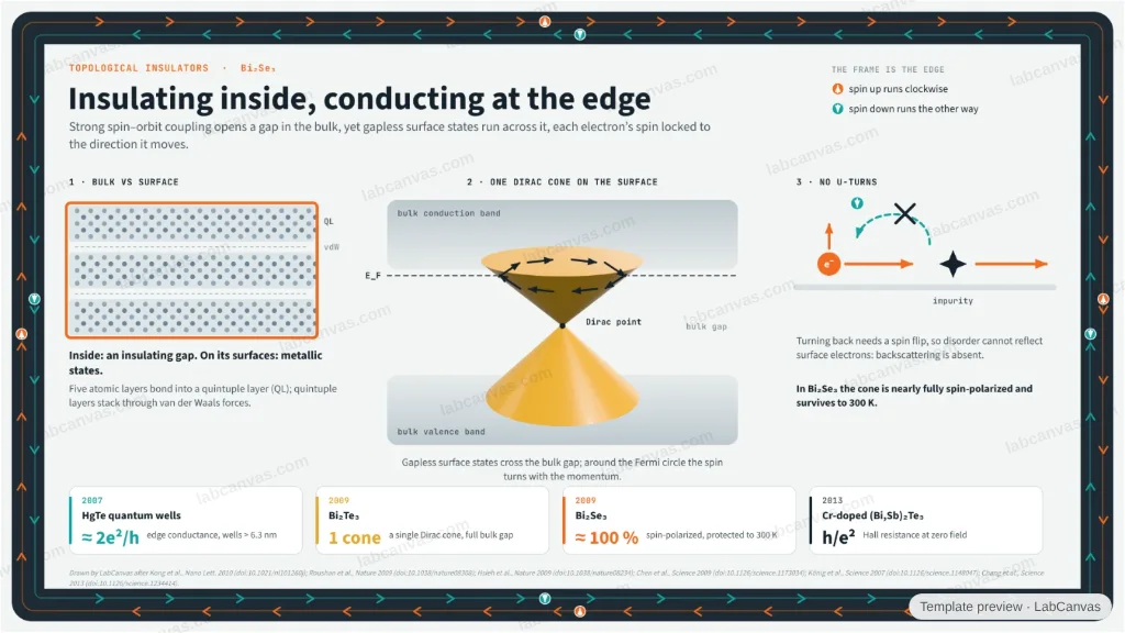
The figure is the insulator: its frame is a two-lane edge channel where spin-up and spin-down electrons travel in opposite directions, while inside a quintuple-layer slab of Bi₂Se₃, a surface Dirac cone crossing the bulk gap (live 3D) and spin–momentum locking explain why the surface conducts and resists backscattering. Four landmark results run along the bottom.
Updated 6 cited papers457 editable layers
At a glance
- Category
- Graphical abstracts
- Method
- Graphical abstract
- Starting materials
- Bi₂Se₃-family crystals: quintuple layers bound by van der Waals forces
- Product
- An insulating bulk wrapped in metallic, spin-polarized surface states
- Key result
- Nearly 100 % spin polarization, protected to 300 K in Bi₂Se₃ (Hsieh et al. 2009); ≈ 2e²/h edge conductance (König et al. 2007); h/e² at zero field (Chang et al. 2013)
- Figure
- 1920 × 1080 px (16:9), 457 editable layers
Step by step
- Bulk vs surfaceA topological insulator has an insulating bulk band gap and metallic surface states (Kong et al. 2010); the gap comes from strong spin–orbit coupling (Roushan et al. 2009)
- One Dirac coneBi₂Se₃, Bi₂Te₃ and Sb₂Te₃ have a single Dirac cone on the surface (Kong et al. 2010; Chen et al. 2009); in Bi₂Se₃ it is spin–momentum locked, nearly 100 % spin-polarized and protected up to 300 K (Hsieh et al. 2009)
- No U-turnsBackscattering between states of opposite momentum and opposite spin is absent even with strong disorder (Roushan et al. 2009)
- LandmarksEdge conductance near 2e²/h in HgTe wells thicker than 6.3 nm (König et al. 2007); quantum anomalous Hall resistance h/e² at zero field in Cr-doped (Bi,Sb)₂Te₃ (Chang et al. 2013)
Uses
- Graphical abstracts on topological insulators and quantum materials
- Talks on spintronics and topological protection
- Teaching band inversion, Dirac cones and spin–momentum locking
Papers this template follows
- Kong et al., “Few-layer nanoplates of Bi2Se3 and Bi2Te3 with highly tunable chemical potential”, Nano Lett. 2010. doi:10.1021/nl101260jprimary
- Roushan et al., “Topological surface states protected from backscattering by chiral spin texture”, Nature 2009. doi:10.1038/nature08308primary
- Hsieh et al., “A tunable topological insulator in the spin helical Dirac transport regime”, Nature 2009. doi:10.1038/nature08234primary
- Chen et al., “Experimental realization of a three-dimensional topological insulator, Bi2Te3”, Science 2009. doi:10.1126/science.1173034primary
- König et al., “Quantum spin Hall insulator state in HgTe quantum wells”, Science 2007. doi:10.1126/science.1148047primary
- Chang et al., “Experimental observation of the quantum anomalous Hall effect in a magnetic topological insulator”, Science 2013. doi:10.1126/science.1234414primary
Drawn by LabCanvas after Kong et al., Nano Lett. 2010 (doi:10.1021/nl101260j); Roushan et al., Nature 2009 (doi:10.1038/nature08308); Hsieh et al., Nature 2009 (doi:10.1038/nature08234); Chen et al., Science 2009 (doi:10.1126/science.1173034); König et al., Science 2007 (doi:10.1126/science.1148047); Chang et al., Science 2013 (doi:10.1126/science.1234414).
How templates are written and checked: editorial guidelines.
Questions
What does the “Topological insulators: insulating inside, conducting at the edge” template show?
The figure is the insulator: its frame is a two-lane edge channel where spin-up and spin-down electrons travel in opposite directions, while inside a quintuple-layer slab of Bi₂Se₃, a surface Dirac cone crossing the bulk gap (live 3D) and spin–momentum locking explain why the surface conducts and resists backscattering. Four landmark results run along the bottom.
What are the steps shown in “Topological insulators: insulating inside, conducting at the edge”?
1. Bulk vs surface: A topological insulator has an insulating bulk band gap and metallic surface states (Kong et al. 2010); the gap comes from strong spin–orbit coupling (Roushan et al. 2009). 2. One Dirac cone: Bi₂Se₃, Bi₂Te₃ and Sb₂Te₃ have a single Dirac cone on the surface (Kong et al. 2010; Chen et al. 2009); in Bi₂Se₃ it is spin–momentum locked, nearly 100 % spin-polarized and protected up to 300 K (Hsieh et al. 2009). 3. No U-turns: Backscattering between states of opposite momentum and opposite spin is absent even with strong disorder (Roushan et al. 2009). 4. Landmarks: Edge conductance near 2e²/h in HgTe wells thicker than 6.3 nm (König et al. 2007); quantum anomalous Hall resistance h/e² at zero field in Cr-doped (Bi,Sb)₂Te₃ (Chang et al. 2013).
What are the starting materials and the product?
Starting materials: Bi₂Se₃-family crystals: quintuple layers bound by van der Waals forces. Product: An insulating bulk wrapped in metallic, spin-polarized surface states.
Which papers is “Topological insulators: insulating inside, conducting at the edge” based on?
Kong et al., “Few-layer nanoplates of Bi2Se3 and Bi2Te3 with highly tunable chemical potential”, Nano Lett. 2010 (doi:10.1021/nl101260j); Roushan et al., “Topological surface states protected from backscattering by chiral spin texture”, Nature 2009 (doi:10.1038/nature08308); Hsieh et al., “A tunable topological insulator in the spin helical Dirac transport regime”, Nature 2009 (doi:10.1038/nature08234); Chen et al., “Experimental realization of a three-dimensional topological insulator, Bi2Te3”, Science 2009 (doi:10.1126/science.1173034); König et al., “Quantum spin Hall insulator state in HgTe quantum wells”, Science 2007 (doi:10.1126/science.1148047); Chang et al., “Experimental observation of the quantum anomalous Hall effect in a magnetic topological insulator”, Science 2013 (doi:10.1126/science.1234414).
Can I edit the “Topological insulators: insulating inside, conducting at the edge” template?
Yes. Open it in the LabCanvas editor: all 457 layers are editable. Change the text, colours and layout, then export PNG, TIFF, SVG or PDF.
Do I need an account to use this template?
Not to view it here. To open and edit it, sign in to LabCanvas or create a free account (the free plan keeps up to 3 designs). Downloading the figure is part of LabCanvas Pro (US$19 a month or US$199 a year).