Hexagonal boron nitride (h-BN): structure, band gap and uses
Hexagonal boron nitride (h-BN) is a layered crystal of boron and nitrogen, BN, built from flat honeycomb sheets like graphene’s but with boron and nitrogen atoms alternating, which makes it an electrical insulator with a wide band gap (an indirect gap of 5.955 eV). Single layers were among the first two-dimensional crystals peeled from bulk crystals (Novoselov et al., PNAS 2005), and since Dean et al. showed in 2010 that graphene on h-BN has mobilities almost an order of magnitude better than on SiO₂, h-BN has been the standard substrate and encapsulating layer for 2D electronics.
Last updated
Hexagonal boron nitride (h-BN) at a glance
| Formula | BN, one boron and one nitrogen per formula unit (from its crystal file) |
|---|---|
| Molar mass | 24.82 g mol⁻¹ (calculated from the formula) |
| Other names | hBN; monolayer h-BN has been called “white graphene” (Song et al. 2010) |
| Layer structure | Flat honeycomb of alternating B and N atoms, each bonded to three of the other kind (from its crystal file) |
| Crystal system | Hexagonal, space group P6₃/mmc, a = 2.504 Å, c = 6.661 Å, two layers per cell (from its crystal file) |
| Layer spacing | 3.33 Å (half the c axis, from its crystal file) |
| Stacking | AA′: each boron sits over a nitrogen in the next layer (from its crystal file) |
| Lattice match with graphene | h-BN’s lattice is 1.8 % larger: 2.504 Å against 2.460 Å (Yankowitz et al. 2012; Liu et al. 2022) |
| Band gap | Indirect, 5.955 eV (Cassabois et al. 2016); few-layer CVD films show an optical gap of 5.5 eV (Song et al. 2010) |
| Ultraviolet emission | Strong luminescence around 215 nm and evidence of room-temperature lasing at 215 nm (Watanabe et al. 2004) |
| As a substrate | Atomically smooth and relatively free of dangling bonds and charge traps; graphene on it has mobilities and carrier inhomogeneity almost an order of magnitude better than on SiO₂ (Dean et al. 2010) |
| Mechanical | 2D modulus of 200–500 N m⁻¹ for 2–5-layer CVD films (Song et al. 2010); monolayer stiffness 289 N m⁻¹, and among the strongest electrically insulating materials (Falin et al. 2017) |
| Oxidation resistance | Monolayer h-BN sustains heating in air up to 850 °C (Li et al. 2014) |
| Protons | Monolayer h-BN is highly permeable to thermal protons, about 10 Ω cm² with an activation energy of about 0.3 eV; multilayer h-BN is not (Hu et al. 2014) |
| Density | About 2.28 g cm⁻³ (calculated from the hexagonal cell) |
| First monolayers | Single layers of boron nitride by micromechanical cleavage: Novoselov et al., PNAS 102, 10451 (2005) |
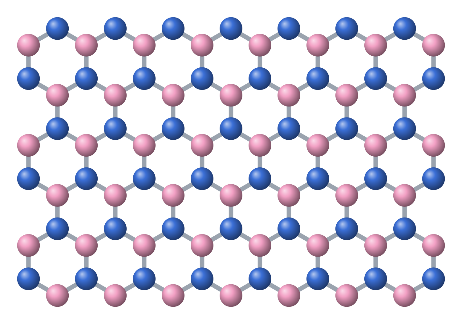
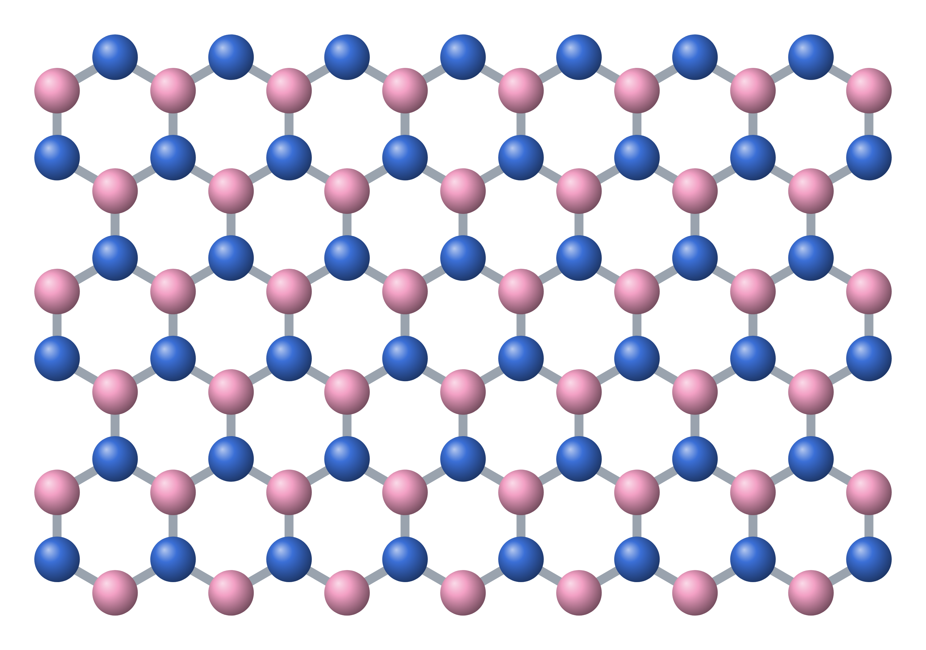
Hexagonal boron nitride (h-BN) structure diagram

Hexagonal boron nitride (h-BN) crystal structure (high-resolution SVG)
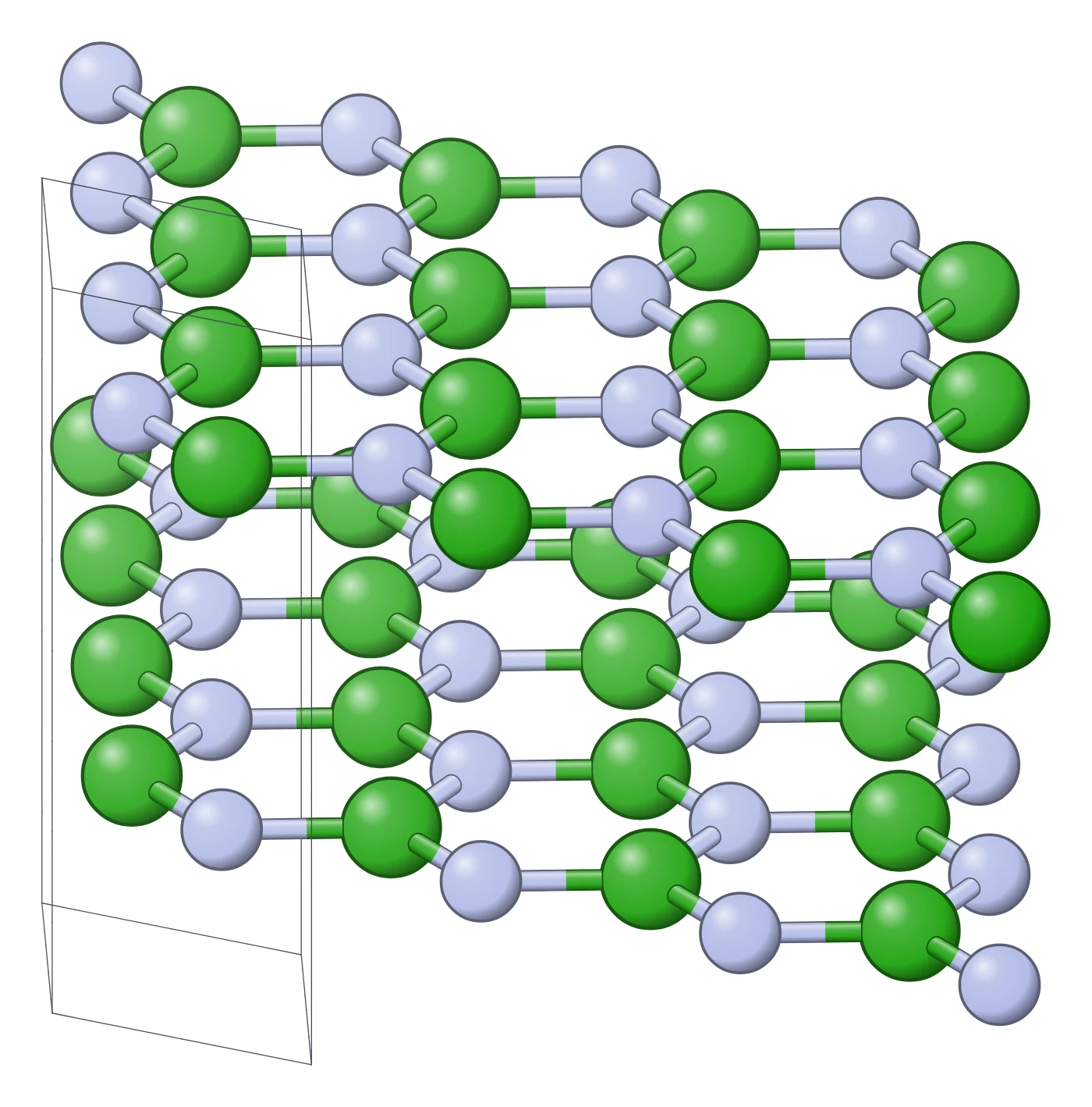
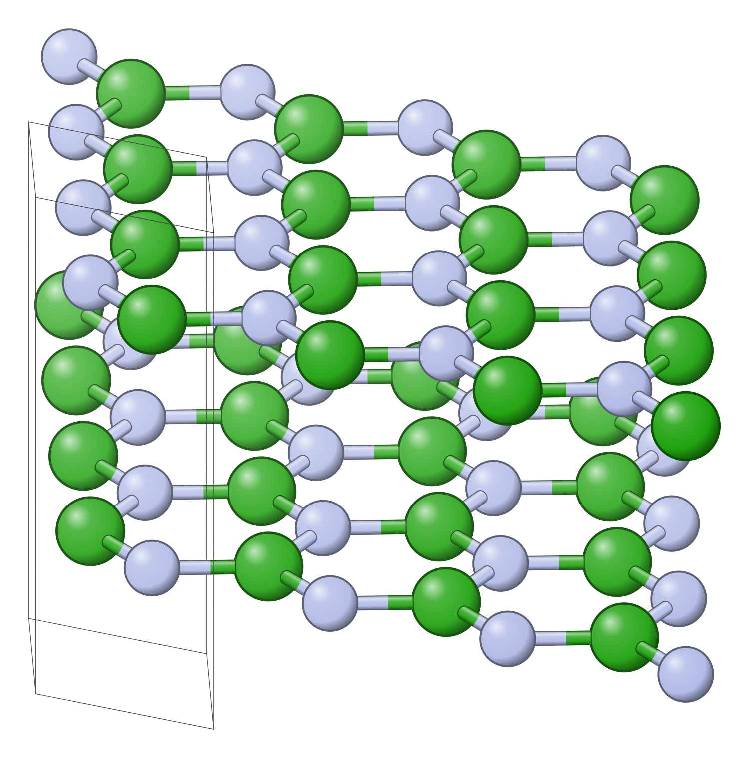
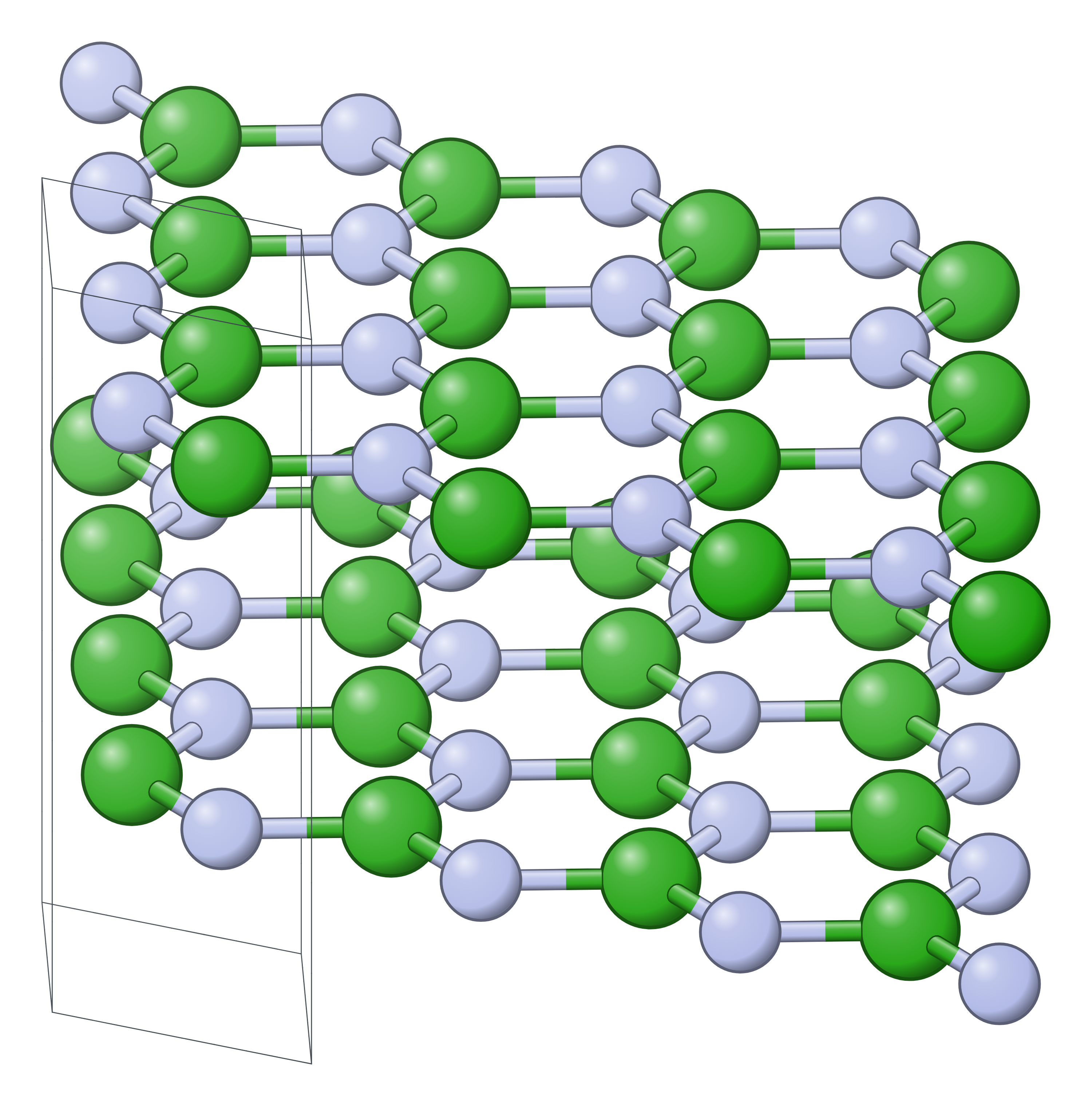
Hexagonal boron nitride (h-BN) structure drawing (high-resolution SVG)
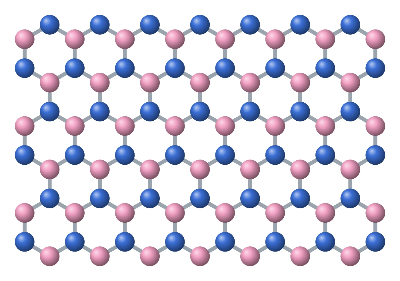
Hexagonal boron nitride (h-BN) in 3D (interactive)
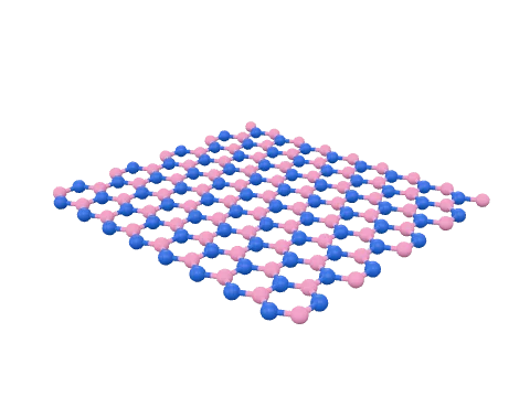
Loading the 3D model…
More Hexagonal boron nitride (h-BN) figures

h-BN structure explained
A single layer of h-BN is a flat honeycomb, like graphene, but its two kinds of corner are occupied by different atoms: every boron is bonded to three nitrogen atoms and every nitrogen to three borons. The lattice constant is 2.504 Å, 1.8 % larger than graphene’s 2.460 Å (Yankowitz et al. 2012; Liu et al. 2022), so the two lattices almost match.
In the bulk crystal the layers are held together by van der Waals forces, 3.33 Å apart. They stack AA′: the hexagons sit directly above one another, but each boron lies over a nitrogen of the next layer, so the cell (hexagonal, P6₃/mmc, a = 2.504 Å, c = 6.661 Å) holds two layers (from its crystal file).
The chemistry changes everything electronic: graphene is a semimetal with no band gap, while h-BN is an insulator with a wide one, measured as an indirect gap of 5.955 eV (Cassabois et al. 2016).
How h-BN is made
- Bulk single crystals. High-purity h-BN crystals are grown under high pressure and high temperature (Watanabe et al. 2004). Flakes from such single crystals were the substrates in the first high-quality graphene-on-h-BN devices (Dean et al. 2010).
- Mechanical exfoliation. Adhesive tape peels thin flakes and single layers off a bulk crystal; boron nitride was among the first 2D crystals made this way (Novoselov et al. 2005). The flakes are then picked up and placed with polymer stamps (Wang et al. 2013; Pizzocchero et al. 2016).
- Chemical vapour deposition. Large-area films two to five atomic layers thick can be grown by CVD (Song et al. 2010).
- Liquid exfoliation. BN, like MoS₂ and other layered compounds, can be dispersed in common solvents into thin flakes and cast into films (Coleman et al. 2011).
Key properties of h-BN
- Wide band gap. An indirect gap of 5.955 eV (Cassabois et al. 2016); few-layer CVD films have an optical gap of 5.5 eV and are highly transparent over a broad wavelength range (Song et al. 2010).
- Deep-ultraviolet light. h-BN crystals luminesce strongly around 215 nm, with evidence of room-temperature lasing at that wavelength (Watanabe et al. 2004).
- A clean, flat surface. Atomically smooth and relatively free of dangling bonds and charge traps, with large optical phonon modes and a large electrical band gap (Dean et al. 2010).
- Strong and stiff. Mono- and few-layer h-BN are among the strongest electrically insulating materials, and unlike graphene their strength hardly changes with the number of layers (Falin et al. 2017).
- Oxidation resistance. Monolayer h-BN survives heating in air up to 850 °C (Li et al. 2014).
- Proton conductor. A single layer lets thermal protons through, with the highest room-temperature proton conductivity of the crystals tested (Hu et al. 2014).
Why h-BN matters
Graphene on the usual SiO₂ substrate is highly disordered. Dean et al. (2010) placed graphene on single-crystal h-BN and found mobilities and carrier inhomogeneity almost an order of magnitude better, with less roughness, doping and chemical reactivity. This made h-BN a widely used substrate for 2D devices.
Wrapping graphene between two h-BN flakes and contacting it only along its edge gave devices with ballistic transport over more than 15 µm at low temperature (Wang et al. 2013), and the same pick-up methods build stacks of h-BN, graphene and other layers in any order: van der Waals heterostructures (Geim & Grigorieva 2013). Graphene aligned on h-BN also forms a moiré superlattice, because of the 1.8 % lattice mismatch (Yankowitz et al. 2012).
Uses and research areas
- Substrate and encapsulation. hBN/graphene/hBN stacks with edge contacts (Wang et al. 2013), made in batches by hot pick-up (Pizzocchero et al. 2016); h-BN-encapsulated MoS₂ transistors are stable even at elevated temperatures (Lee et al. 2015).
- Dielectric layers in heterostructures. A thin, flat insulator between the other layers of van der Waals heterostructures (Dean et al. 2010; Geim & Grigorieva 2013).
- Deep-ultraviolet emitters. Its 215 nm emission made h-BN a candidate for compact ultraviolet lasers (Watanabe et al. 2004).
- Proton-conducting membranes. Monolayer h-BN for hydrogen technologies (Hu et al. 2014).
- High-temperature coatings and reinforcement. Better oxidation resistance than graphene (Li et al. 2014) and good interlayer integrity for mechanical reinforcement (Falin et al. 2017).
How to draw the h-BN structure
For a paper, slide or poster, draw one layer as a honeycomb with two colours of atom (boron and nitrogen alternating), and a side view of two or more layers to show the AA′ stacking and the 3.33 Å spacing. The figures above show h-BN among the other 2D materials and in an encapsulated graphene stack, and open as editable LabCanvas figures. The structure drawing is a high-resolution SVG of a single h-BN layer that opens in the LabCanvas figure editor. The crystal structure drawing is a high-resolution SVG from the h-BN crystal file and opens in the figure editor, where you can change the style, the number of cells and the view. The 3D model opens in the LabCanvas 3D Studio, where you can stack layers, change the stacking and export a high-resolution image.
h-BN compared with other 2D materials
| Material | Composition | One layer | Electronic character | Usually made by | Key report |
|---|---|---|---|---|---|
| Graphene | C | Flat honeycomb of carbon | Semimetal, no band gap | Tape exfoliation of graphite; CVD | Novoselov et al., Science 2004 |
| Graphene oxide | C, O, H | Graphene sheet carrying oxygen groups | Insulating; reduction (rGO) restores much of the conductivity | Oxidizing graphite (Hummers method) | Hummers & Offeman, JACS 1958 |
| h-BN | BN | Flat honeycomb of alternating B and N | Insulator, indirect gap 5.955 eV | Exfoliating high-pressure crystals; CVD | Dean et al., Nat. Nanotechnol. 2010 |
| MoS₂ (2H) | MoS₂ | S–Mo–S sandwich, Mo in trigonal prisms | Semiconductor; direct 1.8 eV gap as one layer | Exfoliation; CVD | Mak et al., PRL 2010 |
| MXene (Ti₃C₂Tₓ) | Ti₃C₂ with –O, –OH, –F | Ti–C–Ti–C–Ti, both faces terminated | Metallic; films 4,600 S cm⁻¹ | Etching Al out of Ti₃AlC₂ | Naguib et al., Adv. Mater. 2011 |
Related materials
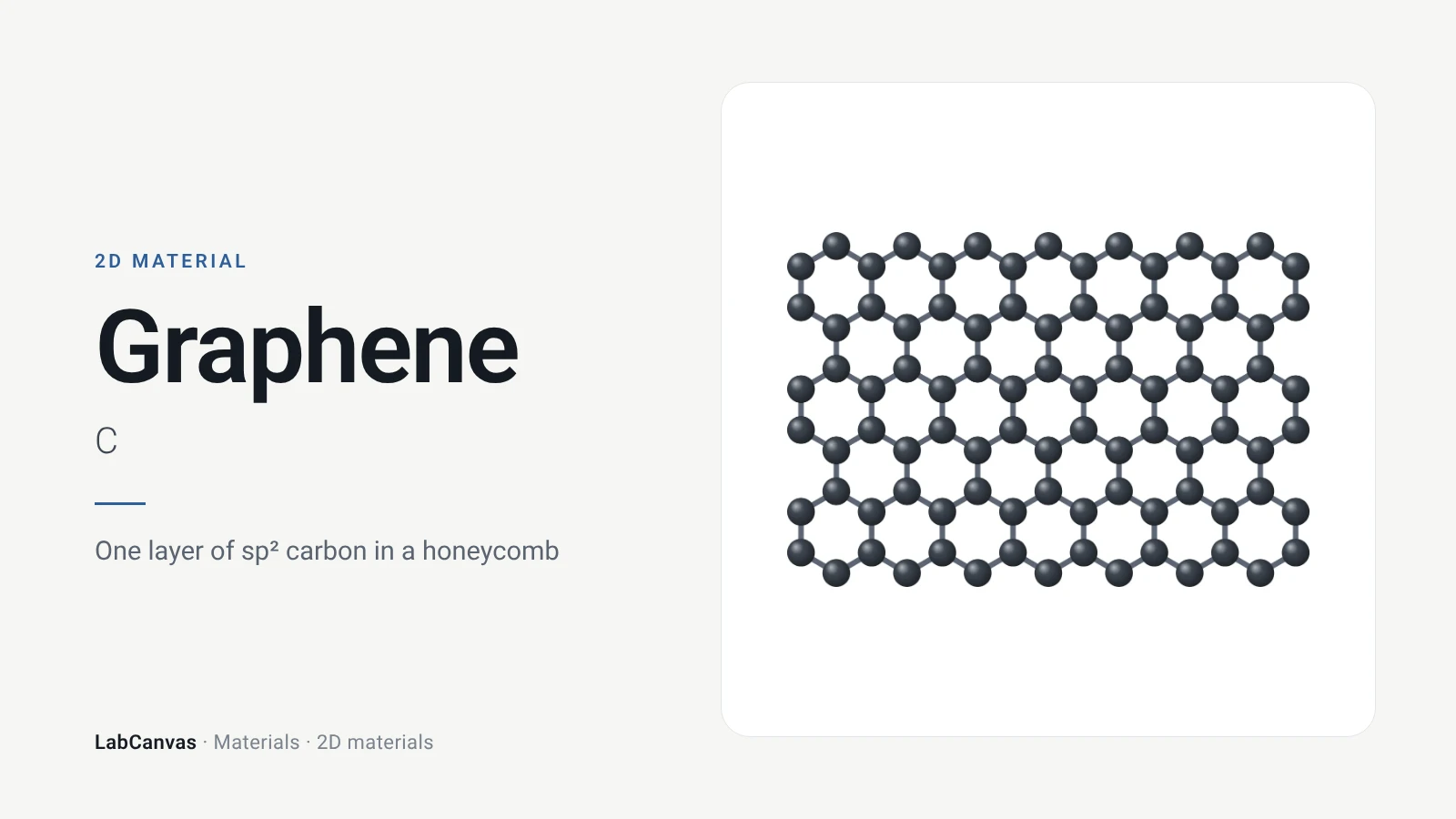
Graphene
Graphene structure explained: the one-atom-thick honeycomb of sp² carbon, its Dirac bands, strength and conductivity, how it is made and used. Cited facts.
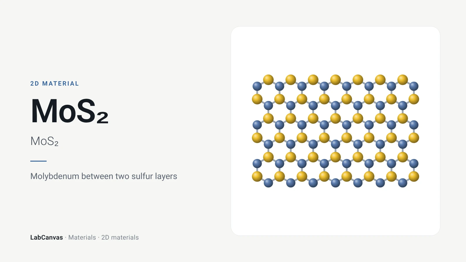
MoS₂ (molybdenum disulfide)
MoS₂ structure and band gap: the S–Mo–S layer, 2H and 1T phases, the 1.8 eV direct gap of monolayer MoS₂, transistors and HER catalysis. Editable figures.
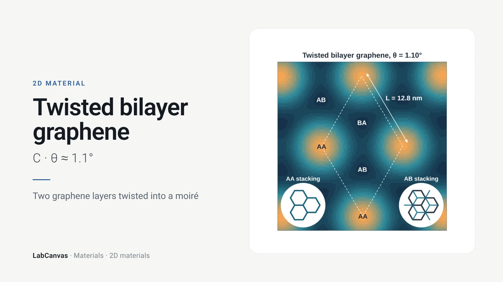
Twisted bilayer graphene
Twisted bilayer graphene explained: two layers turned by a small angle, the moiré, the 1.1° magic angle, flat bands and superconductivity. Cited papers.
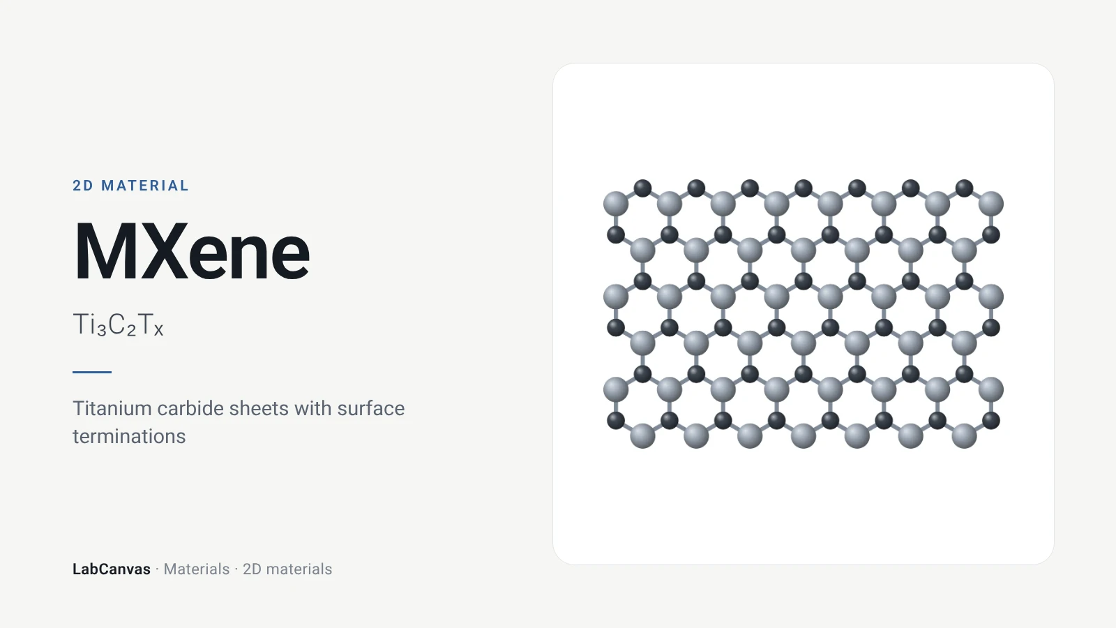
MXene (Ti₃C₂Tₓ)
MXene Ti₃C₂Tₓ explained: 2D titanium carbide etched from the MAX phase Ti₃AlC₂, its surface terminations, synthesis, conductivity and uses. Editable figures.
More on LabCanvas
- The graphene family of 2D materials: Editable figure template
- Graphene transfer methods compared: Editable figure template
- More figure templates in this category: Ready-made, cited figures to edit
- Crystal structure figure software compared: VESTA, Mercury, CrystalMaker, Avogadro and LabCanvas
- XRD Scherrer crystallite size calculator: Free tool
- Molar mass calculator: Free tool
- Journal figure size guide: Column widths and resolutions for 38 journals
- 3D models gallery: Turn MOFs, COFs and more in 3D
Frequently asked questions
What is hexagonal boron nitride (h-BN)?
A layered crystal of boron and nitrogen (BN) made of flat honeycomb sheets, like graphite, but with boron and nitrogen alternating. It is an electrical insulator with a wide band gap, and single layers of it are a 2D material used as the substrate and protective layer for graphene and other 2D devices.
Why is h-BN called white graphene?
Because it has graphene’s honeycomb structure but, as a wide-gap insulator, it is transparent rather than black: few-layer h-BN films are highly transparent over a broad range of wavelengths. Monolayer h-BN has been called “white graphene” in the research literature (Song et al., Nano Lett. 2010).
What is the band gap of h-BN?
About 6 eV. Optical spectroscopy gives an indirect band gap of 5.955 eV (Cassabois et al., Nat. Photonics 2016); h-BN crystals emit deep-ultraviolet light around 215 nm (Watanabe et al., Nat. Mater. 2004), and few-layer CVD films show an optical gap of 5.5 eV (Song et al. 2010).
What is the structure of h-BN?
Flat honeycomb layers of alternating B and N atoms, 3.33 Å apart, stacked AA′ with boron over nitrogen. The crystal is hexagonal, space group P6₃/mmc, with a = 2.504 Å and c = 6.661 Å (two layers per cell).
Is h-BN a conductor or an insulator?
An insulator. Its wide band gap (5.955 eV, indirect) means it does not conduct electricity, which is why it is used as a dielectric, gate insulator and encapsulating layer in 2D devices.
Why is h-BN used as a substrate for graphene?
It is atomically smooth, relatively free of dangling bonds and charge traps, and its lattice is only 1.8 % larger than graphene’s. Graphene on h-BN has mobilities and carrier inhomogeneity almost an order of magnitude better than on SiO₂ (Dean et al., Nat. Nanotechnol. 2010).
How is h-BN made?
Bulk single crystals are grown at high pressure and high temperature (Watanabe et al. 2004) and peeled into thin flakes with tape. Large-area films of a few layers are grown by chemical vapour deposition (Song et al. 2010), and BN can also be exfoliated in solvents (Coleman et al. 2011).
What is the difference between h-BN and graphene?
Both are flat honeycombs with almost the same lattice constant (2.504 and 2.460 Å), but graphene is all carbon and a semimetal with no band gap, while h-BN alternates boron and nitrogen and is an insulator with a band gap of about 6 eV. They are often used together: graphene on or between layers of h-BN.
How can I draw h-BN for a paper or presentation?
Open the figures on this page in LabCanvas (free) to edit them, add the h-BN layer drawing or the crystal structure in the figure editor, or open the 3D model in the LabCanvas 3D Studio and export a render.
References
- C. R. Dean et al.. Boron nitride substrates for high-quality graphene electronics. Nat. Nanotechnol. 2010, 5, 722–726. doi:10.1038/nnano.2010.172
- K. Watanabe, T. Taniguchi, H. Kanda. Direct-bandgap properties and evidence for ultraviolet lasing of hexagonal boron nitride single crystal. Nat. Mater. 2004, 3, 404–409. doi:10.1038/nmat1134
- G. Cassabois, P. Valvin, B. Gil. Hexagonal boron nitride is an indirect bandgap semiconductor. Nat. Photonics 2016, 10, 262–266. doi:10.1038/nphoton.2015.277
- K. S. Novoselov et al.. Two-dimensional atomic crystals. Proc. Natl. Acad. Sci. USA 2005, 102, 10451–10453. doi:10.1073/pnas.0502848102
- L. Song et al.. Large scale growth and characterization of atomic hexagonal boron nitride layers. Nano Lett. 2010, 10, 3209–3215. doi:10.1021/nl1022139
- A. Falin et al.. Mechanical properties of atomically thin boron nitride and the role of interlayer interactions. Nat. Commun. 2017, 8, 15815. doi:10.1038/ncomms15815
- L. H. Li, J. Cervenka, K. Watanabe, T. Taniguchi, Y. Chen. Strong oxidation resistance of atomically thin boron nitride nanosheets. ACS Nano 2014, 8, 1457–1462. doi:10.1021/nn500059s
- S. Hu et al.. Proton transport through one-atom-thick crystals. Nature 2014, 516, 227–230. doi:10.1038/nature14015
- L. Wang et al.. One-dimensional electrical contact to a two-dimensional material. Science 2013, 342, 614–617. doi:10.1126/science.1244358
- F. Pizzocchero et al.. The hot pick-up technique for batch assembly of van der Waals heterostructures. Nat. Commun. 2016, 7, 11894. doi:10.1038/ncomms11894
- A. K. Geim, I. V. Grigorieva. Van der Waals heterostructures. Nature 2013, 499, 419–425. doi:10.1038/nature12385
- M. Yankowitz et al.. Emergence of superlattice Dirac points in graphene on hexagonal boron nitride. Nat. Phys. 2012, 8, 382. doi:10.1038/nphys2272
- X. Liu et al.. Influence of hexagonal boron nitride on electronic structure of graphene. Molecules 2022, 27, 3740. doi:10.3390/molecules27123740
- J. N. Coleman et al.. Two-dimensional nanosheets produced by liquid exfoliation of layered materials. Science 2011, 331, 568–571. doi:10.1126/science.1194975
- G.-H. Lee et al.. Highly stable, dual-gated MoS₂ transistors encapsulated by hexagonal boron nitride with gate-controllable contact, resistance, and threshold voltage. ACS Nano 2015, 9, 7019–7026. doi:10.1021/acsnano.5b01341
- K. S. Novoselov et al.. Electric field effect in atomically thin carbon films. Science 2004, 306, 666–669. doi:10.1126/science.1102896
- K. F. Mak, C. Lee, J. Hone, J. Shan, T. F. Heinz. Atomically thin MoS₂: a new direct-gap semiconductor. Phys. Rev. Lett. 2010, 105, 136805. doi:10.1103/PhysRevLett.105.136805
- M. Naguib et al.. Two-dimensional nanocrystals produced by exfoliation of Ti₃AlC₂. Adv. Mater. 2011, 23, 4248–4253. doi:10.1002/adma.201102306
- W. S. Hummers, R. E. Offeman. Preparation of graphitic oxide. J. Am. Chem. Soc. 1958, 80, 1339. doi:10.1021/ja01539a017
Draw Hexagonal boron nitride (h-BN) for your paper or slides
LabCanvas is a browser workspace for scientific figures: framework clusters, linkers and nets, crystal structures in 2D and 3D, graphs and posters, all editable.
Edit the Hexagonal boron nitride (h-BN) figure