MoS₂ (molybdenum disulfide): structure, band gap and uses
Molybdenum disulfide (MoS₂) is a layered transition metal dichalcogenide: each layer is a sandwich of molybdenum atoms between two sheets of sulfur (S–Mo–S), and in the common 2H form the layers repeat every 6.15 Å. Bulk MoS₂, the mineral molybdenite, is an indirect-gap semiconductor; thinned to one layer it becomes a direct-gap semiconductor that emits light strongly, as Mak et al. and Splendiani et al. reported in 2010. Its 1.8 eV gap let Radisavljevic et al. build single-layer MoS₂ transistors in 2011 with on/off ratios of 10⁸.
Last updated
MoS₂ (molybdenum disulfide) at a glance
| Formula | MoS₂ (from its crystal file) |
|---|---|
| Molar mass | 160.07 g mol⁻¹ (calculated from the formula) |
| Class | Layered transition metal dichalcogenide (TMD) (Wang et al. 2012) |
| Layer structure | S–Mo–S sandwich; in 2H-MoS₂ each Mo sits in a trigonal prism of six S (Wang et al. 2014) |
| Crystal system | 2H: hexagonal, space group P6₃/mmc, a = 3.16 Å, c = 12.29 Å, two layers per cell (from its crystal file) |
| Mo–S bond | 2.42 Å (from its crystal file) |
| Layer spacing | 6.15 Å (half the c axis, from its crystal file) |
| Other phase | 1T: Mo in octahedral coordination, metallic (Wang et al. 2014; Voiry et al. 2013; Acerce et al. 2015) |
| Band gap, bulk | Indirect; as the crystal is thinned the indirect gap moves up by more than 0.6 eV (Mak et al. 2010) |
| Band gap, monolayer | Direct, 1.8 eV (Mak et al. 2010; Radisavljevic et al. 2011) |
| Photoluminescence | Strong in the monolayer: luminescence quantum efficiency more than 10⁴ times that of the bulk (Mak et al. 2010) |
| Transistor | Single layer with an HfO₂ gate: mobility of at least 200 cm² V⁻¹ s⁻¹ and on/off ratio of 10⁸ at room temperature (Radisavljevic et al. 2011) |
| Catalysis | Hydrogen evolution at the layer edges: activity linear in the number of edge sites (Jaramillo et al. 2007); 0.1–0.2 V overpotential for nanoparticles on graphite (Hinnemann et al. 2005) |
| Density | About 5.00 g cm⁻³ (calculated from the 2H cell) |
| Key reports | Mak et al., Phys. Rev. Lett. 105, 136805 (2010); Splendiani et al., Nano Lett. 10, 1271 (2010); Radisavljevic et al., Nat. Nanotechnol. 6, 147 (2011) |
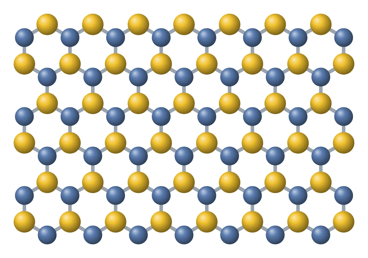
MoS₂ (molybdenum disulfide) structure diagram
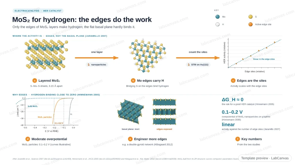
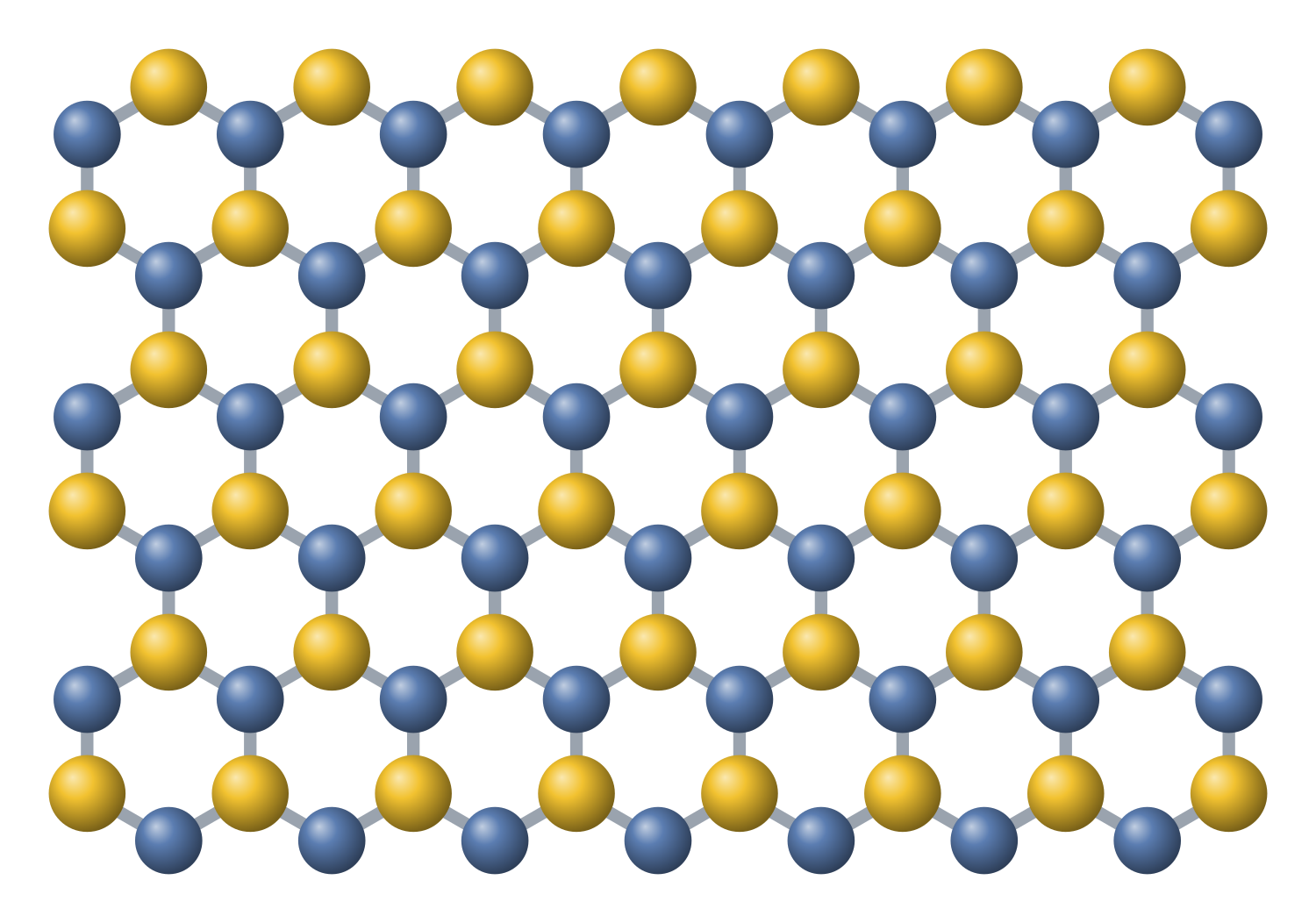
MoS₂ (molybdenum disulfide) crystal structure (high-resolution SVG)
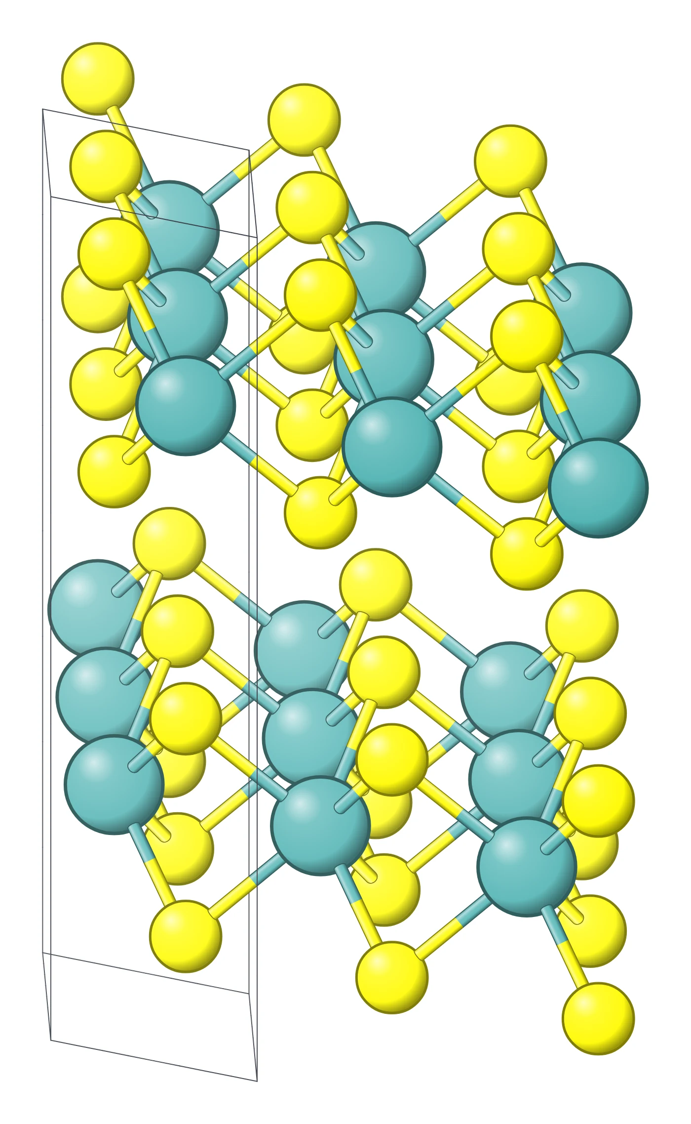
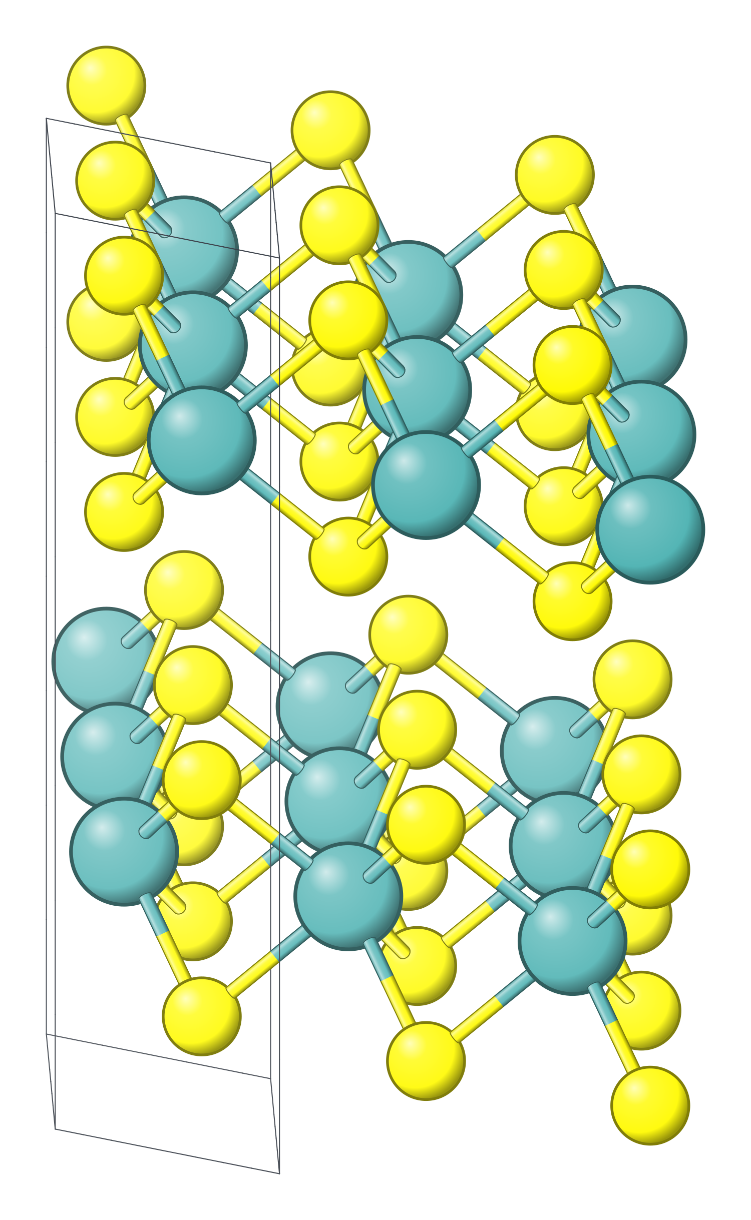
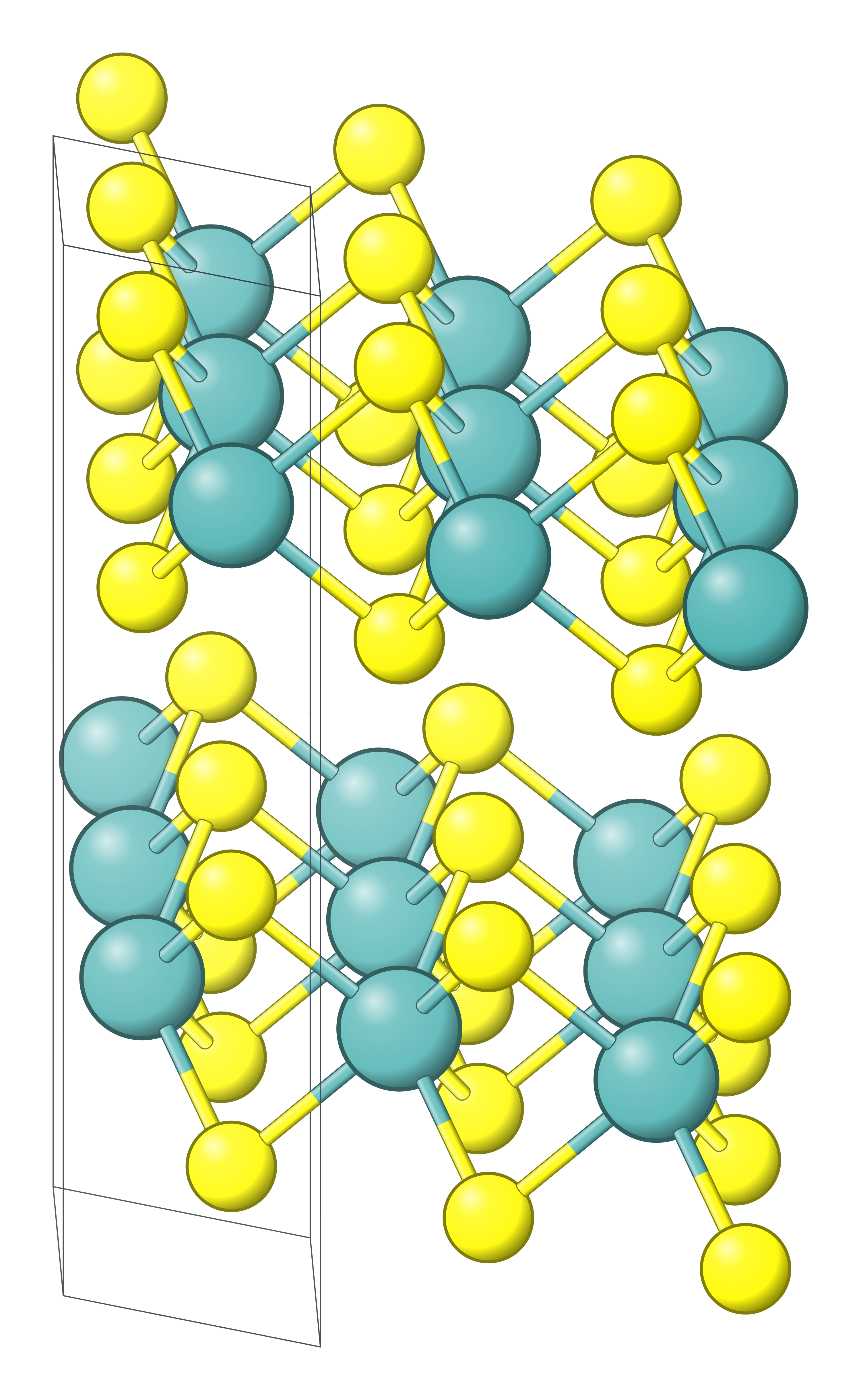
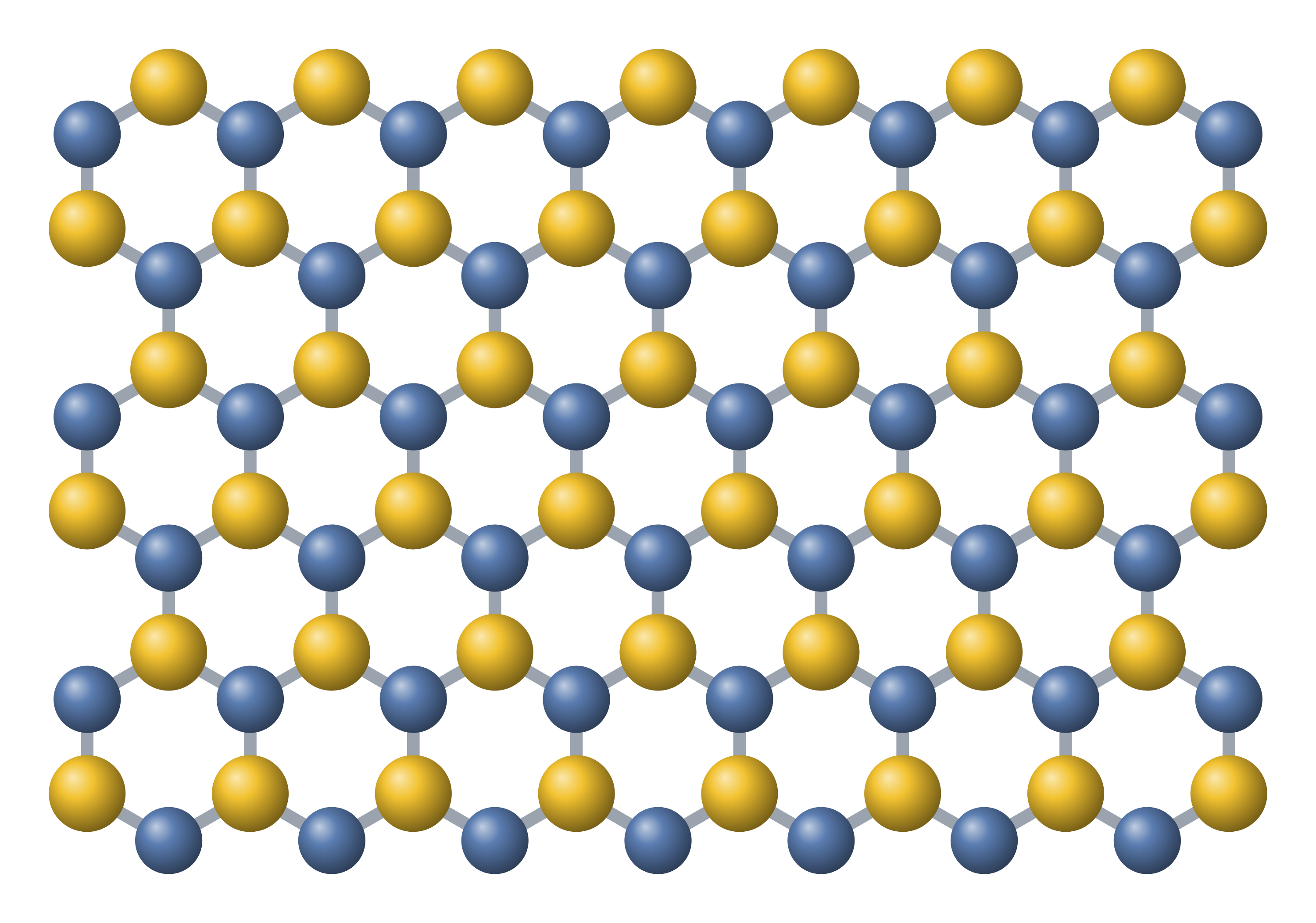
MoS₂ (molybdenum disulfide) structure drawing (high-resolution SVG)
MoS₂ (molybdenum disulfide) in 3D (interactive)
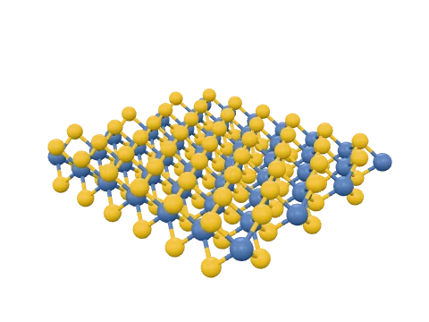
Loading the 3D model…
More MoS₂ (molybdenum disulfide) figures

MoS₂ structure explained
One MoS₂ layer is three atomic planes thick: a plane of molybdenum between two planes of sulfur. Each Mo is bonded to six S atoms (Mo–S 2.42 Å) and each S to three Mo, so the layer is held together by strong bonds within itself, while neighbouring layers are held only by van der Waals forces.
In the common 2H form the sulfur atoms above and below each Mo sit directly over one another, so Mo is in a trigonal prism; in the 1T form the two sulfur sheets sit over different sites, so Mo is in an octahedron (Wang et al. 2014). 2H-MoS₂ is a semiconductor; 1T-MoS₂ is metallic (Voiry et al. 2013; Acerce et al. 2015).
Bulk 2H-MoS₂, the mineral molybdenite, is hexagonal (P6₃/mmc, a = 3.16 Å, c = 12.29 Å) with two layers per cell, so the layers repeat every 6.15 Å (from its crystal file).
How MoS₂ is made
- Mechanical exfoliation. Tape peels single layers off bulk crystals; several dichalcogenides were among the first 2D crystals isolated this way (Novoselov et al. 2005).
- Liquid exfoliation. MoS₂ disperses in common solvents into thin flakes that can be deposited individually or formed into films and composites (Coleman et al. 2011).
- Chemical exfoliation. Chemically exfoliated nanosheets contain a high concentration of the metallic 1T phase (Acerce et al. 2015).
- Chemical vapour deposition. Single-layer MoS₂ grows from vapour on a substrate, with grains that meet at grain boundaries (Najmaei et al. 2013); continuous monolayers have been grown at atmospheric pressure at 750 °C (Prasad & Singh 2023).
Key properties of MoS₂
- Band gap that depends on thickness. As MoS₂ is thinned from six layers to one, its indirect gap moves up by more than 0.6 eV until, in the monolayer, the gap becomes direct (Mak et al. 2010; Splendiani et al. 2010). The monolayer gap is 1.8 eV (Radisavljevic et al. 2011).
- Light emission. Bulk MoS₂ has negligible photoluminescence; the monolayer emits strongly, with a quantum efficiency more than 10⁴ times higher (Mak et al. 2010; Splendiani et al. 2010).
- Transistor action. A single layer with a hafnium oxide gate reached a room-temperature mobility of at least 200 cm² V⁻¹ s⁻¹ and on/off ratios of 10⁸ (Radisavljevic et al. 2011); how that mobility was extracted was later debated in the same journal (Radisavljevic & Kis 2013). h-BN-encapsulated devices gave two-terminal mobilities of 33–151 cm² V⁻¹ s⁻¹ (Lee et al. 2015).
- Catalytic edges. The edges of the layers evolve hydrogen; the flat basal plane is inert (Jaramillo et al. 2007; Kibsgaard et al. 2012).
- Piezoelectric single layers. Single-atomic-layer MoS₂ is piezoelectric (Wu et al. 2014).
Why MoS₂ matters
Graphene has no band gap, so a graphene transistor never switches fully off. Single-layer MoS₂ has a large intrinsic gap of 1.8 eV, and its transistors switched with on/off ratios of 10⁸ and very low standby power (Radisavljevic et al. 2011). Together with the discovery that the monolayer gap is direct (Mak et al. 2010; Splendiani et al. 2010), this put MoS₂ at the centre of research on 2D transition metal dichalcogenides for electronics and optoelectronics (Wang et al. 2012).
In catalysis MoS₂ showed that a cheap, earth-abundant sulfide can evolve hydrogen at a moderate overpotential (Hinnemann et al. 2005), and that the activity comes from the edges (Jaramillo et al. 2007), so MoS₂ catalysts are now engineered to expose as many edges as possible (Kibsgaard et al. 2012).
Uses and research areas
- Transistors and logic. Single-layer and few-layer MoS₂ channels (Radisavljevic et al. 2011; Wang et al. 2012).
- Optoelectronics. Light emission and absorption from the direct-gap monolayer (Mak et al. 2010; Wang et al. 2012).
- Hydrogen evolution. Edge-rich nanoparticles and double-gyroid films (Jaramillo et al. 2007; Kibsgaard et al. 2012), and conducting 1T-MoS₂ nanosheets (Voiry et al. 2013).
- Supercapacitors. 1T-rich MoS₂ nanosheets reach about 400–700 F cm⁻³ in aqueous electrolytes (Acerce et al. 2015).
- Composites and heterostructures. MoS₂ flakes reinforce polymers (Coleman et al. 2011) and are stacked with graphene and h-BN in van der Waals heterostructures (Geim & Grigorieva 2013).
How to draw the MoS₂ structure
For a paper, slide or poster, show a top view of the hexagonal lattice and a side view of the S–Mo–S sandwich, with the trigonal prisms of 2H-MoS₂ (or the octahedra of 1T) drawn as polyhedra if coordination matters. The figures above show MoS₂ as a catalyst and among the other 2D materials, and open as editable LabCanvas figures. The structure drawing is a high-resolution SVG of one layer seen side on that opens in the LabCanvas figure editor. The crystal structure drawing is a high-resolution SVG from the 2H-MoS₂ crystal file and opens in the figure editor, where you can change the style, the number of cells and the view. The 3D model opens in the LabCanvas 3D Studio, where you can switch between 2H and 1T, show the polyhedra and export a high-resolution image.
MoS₂ compared with other 2D materials
| Material | Composition | One layer | Electronic character | Usually made by | Key report |
|---|---|---|---|---|---|
| Graphene | C | Flat honeycomb of carbon | Semimetal, no band gap | Tape exfoliation of graphite; CVD | Novoselov et al., Science 2004 |
| Graphene oxide | C, O, H | Graphene sheet carrying oxygen groups | Insulating; reduction (rGO) restores much of the conductivity | Oxidizing graphite (Hummers method) | Hummers & Offeman, JACS 1958 |
| h-BN | BN | Flat honeycomb of alternating B and N | Insulator, indirect gap 5.955 eV | Exfoliating high-pressure crystals; CVD | Dean et al., Nat. Nanotechnol. 2010 |
| MoS₂ (2H) | MoS₂ | S–Mo–S sandwich, Mo in trigonal prisms | Semiconductor; direct 1.8 eV gap as one layer | Exfoliation; CVD | Mak et al., PRL 2010 |
| MXene (Ti₃C₂Tₓ) | Ti₃C₂ with –O, –OH, –F | Ti–C–Ti–C–Ti, both faces terminated | Metallic; films 4,600 S cm⁻¹ | Etching Al out of Ti₃AlC₂ | Naguib et al., Adv. Mater. 2011 |
Related materials
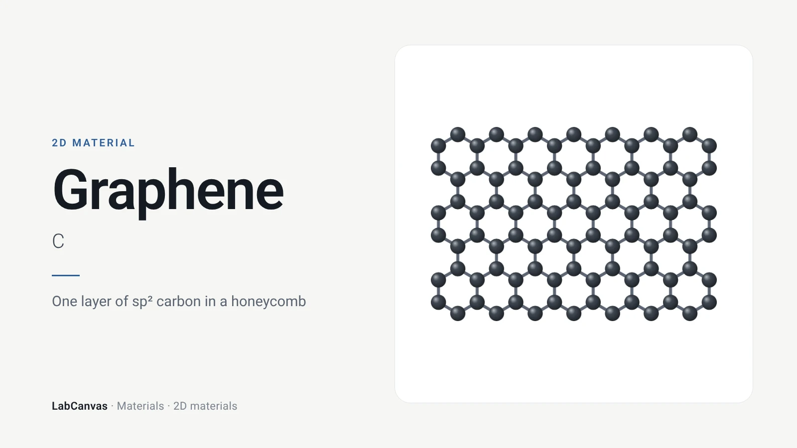
Graphene
Graphene structure explained: the one-atom-thick honeycomb of sp² carbon, its Dirac bands, strength and conductivity, how it is made and used. Cited facts.
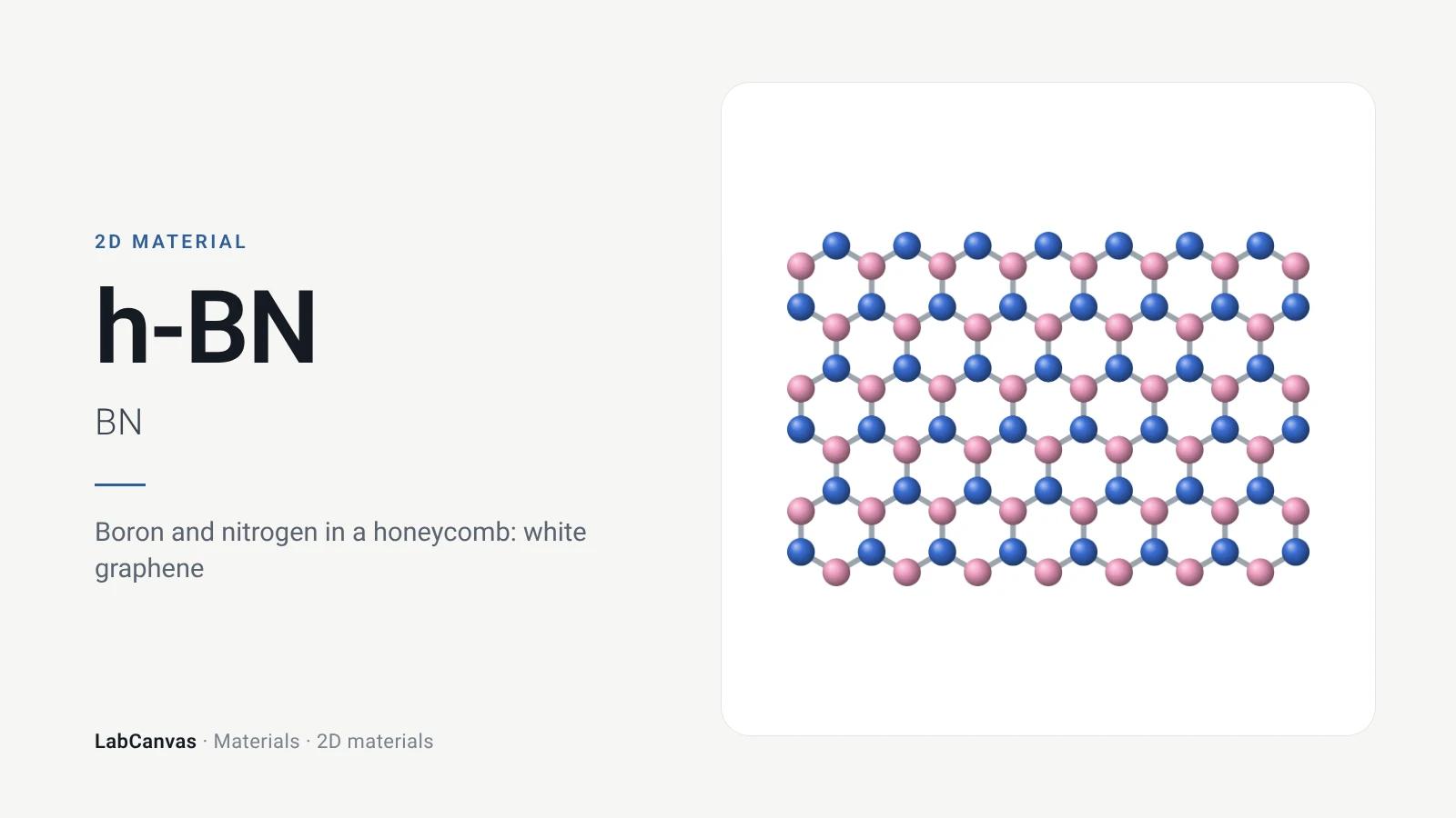
Hexagonal boron nitride (h-BN)
Hexagonal boron nitride (h-BN), “white graphene”: its B–N honeycomb structure, ~6 eV band gap, how it is made and why 2D devices sit on it. Editable figures.
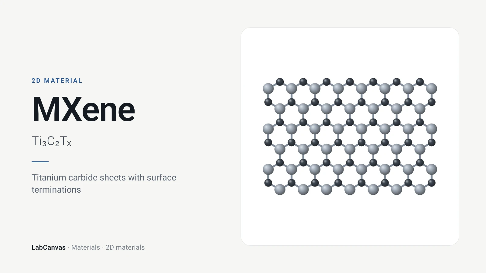
MXene (Ti₃C₂Tₓ)
MXene Ti₃C₂Tₓ explained: 2D titanium carbide etched from the MAX phase Ti₃AlC₂, its surface terminations, synthesis, conductivity and uses. Editable figures.
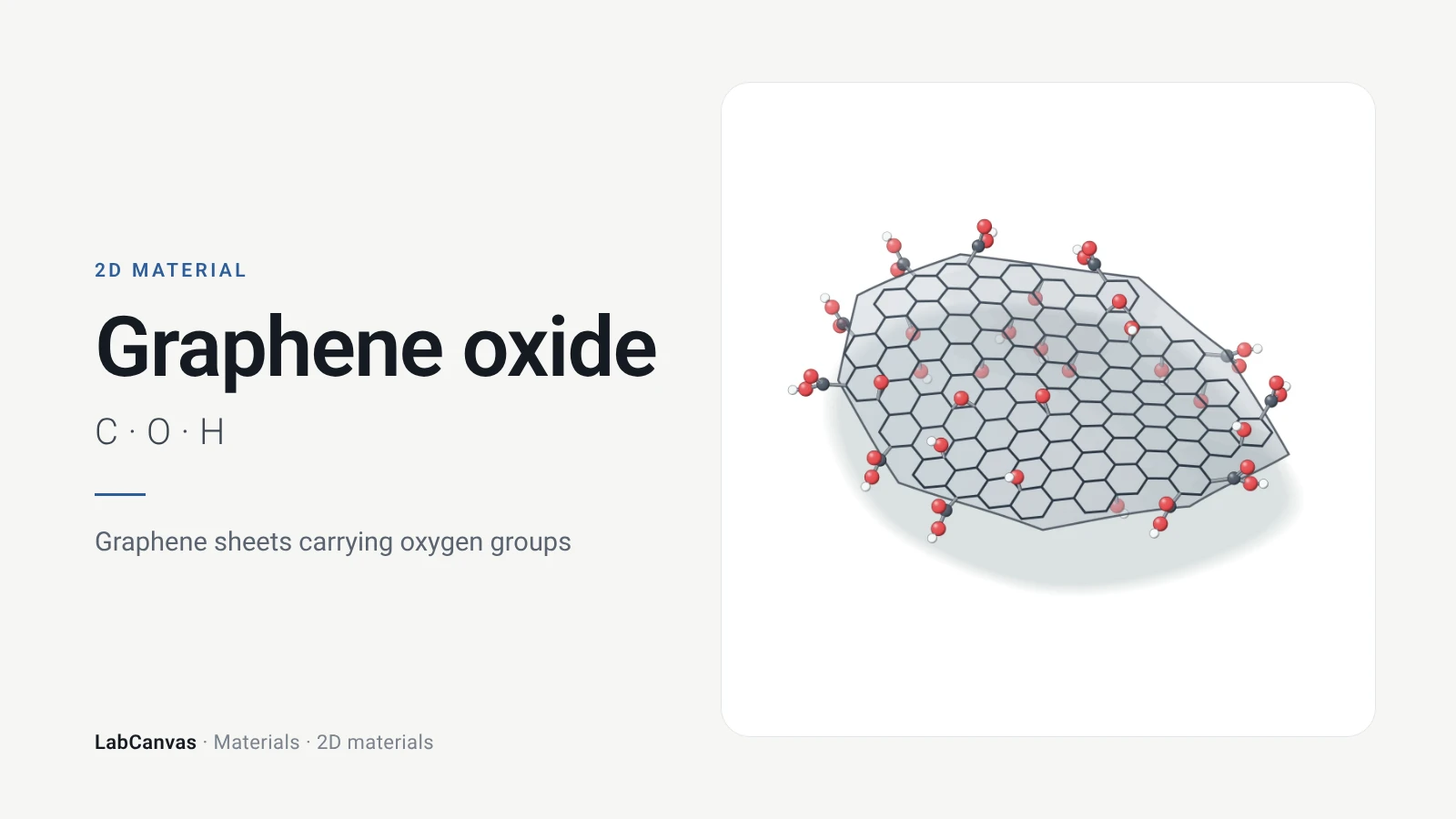
Graphene oxide
Graphene oxide structure explained: graphene with epoxide, hydroxyl and carboxyl groups, made by the Hummers method and reduced to rGO. Cited facts, figures.
More on LabCanvas
- MoS₂ for hydrogen: the edges do the work: Editable figure template
- The graphene family of 2D materials: Editable figure template
- More figure templates in this category: Ready-made, cited figures to edit
- More figure templates in this category: Ready-made, cited figures to edit
- Crystal structure figure software compared: VESTA, Mercury, CrystalMaker, Avogadro and LabCanvas
- XRD Scherrer crystallite size calculator: Free tool
- Molar mass calculator: Free tool
- Journal figure size guide: Column widths and resolutions for 38 journals
- 3D models gallery: Turn MOFs, COFs and more in 3D
Frequently asked questions
What is MoS₂?
Molybdenum disulfide, a layered transition metal dichalcogenide found in nature as the mineral molybdenite. Each layer is a sandwich of molybdenum between two sheets of sulfur; single layers are a 2D semiconductor used in transistors, optoelectronics and hydrogen evolution catalysts.
What is the band gap of MoS₂?
Monolayer MoS₂ has a direct band gap of 1.8 eV (Mak et al., PRL 2010; Radisavljevic et al., Nat. Nanotechnol. 2011). Bulk MoS₂ has a smaller, indirect gap: as the crystal is thinned the indirect gap moves up by more than 0.6 eV until it crosses over to direct in the single layer.
Is MoS₂ a direct or indirect band gap semiconductor?
Both, depending on thickness: bulk and few-layer MoS₂ have an indirect gap, and a single layer has a direct gap. That is why monolayer MoS₂ emits light strongly while the bulk crystal barely luminesces (Mak et al. 2010; Splendiani et al. 2010).
What is the crystal structure of MoS₂?
The common 2H form is hexagonal, space group P6₃/mmc, with a = 3.16 Å and c = 12.29 Å: S–Mo–S layers, Mo in trigonal prisms of sulfur, two layers per cell and a layer repeat of 6.15 Å.
What is the difference between 2H and 1T MoS₂?
In 2H-MoS₂ each molybdenum sits in a trigonal prism of sulfur and the material is a semiconductor; in 1T-MoS₂ it sits in an octahedron and the material is metallic (Wang et al. 2014; Voiry et al. 2013). Chemically exfoliated 1T-rich sheets are used as catalysts and supercapacitor electrodes.
How thick is a MoS₂ monolayer?
One layer is three atomic planes, S–Mo–S. In the bulk crystal the layers repeat every 6.15 Å (half the c axis of 2H-MoS₂).
Why is MoS₂ a good catalyst for hydrogen evolution?
A good hydrogen evolution catalyst binds hydrogen with a free energy close to zero; on that criterion MoS₂ nanoparticles were identified as a promising catalyst and evolved hydrogen at a moderate overpotential of 0.1–0.2 V (Hinnemann et al. 2005). The activity scales with the number of edge sites, not the area: the edges are the active sites and the basal plane is inert (Jaramillo et al., Science 2007; Kibsgaard et al. 2012).
What is the mobility of a MoS₂ transistor?
The first single-layer MoS₂ transistors, with a hafnium oxide gate, reported at least 200 cm² V⁻¹ s⁻¹ at room temperature and on/off ratios of 10⁸ (Radisavljevic et al. 2011); the way that mobility was extracted was later debated. h-BN-encapsulated devices gave two-terminal mobilities of 33–151 cm² V⁻¹ s⁻¹ (Lee et al. 2015).
How is monolayer MoS₂ made?
By peeling flakes off bulk crystals with tape, by exfoliating MoS₂ in solvents (Coleman et al. 2011) or chemically, or by chemical vapour deposition on a substrate (Najmaei et al. 2013).
References
- K. F. Mak, C. Lee, J. Hone, J. Shan, T. F. Heinz. Atomically thin MoS₂: a new direct-gap semiconductor. Phys. Rev. Lett. 2010, 105, 136805. doi:10.1103/PhysRevLett.105.136805
- A. Splendiani et al.. Emerging photoluminescence in monolayer MoS₂. Nano Lett. 2010, 10, 1271–1275. doi:10.1021/nl903868w
- B. Radisavljevic, A. Radenovic, J. Brivio, V. Giacometti, A. Kis. Single-layer MoS₂ transistors. Nat. Nanotechnol. 2011, 6, 147–150. doi:10.1038/nnano.2010.279
- B. Radisavljevic, A. Kis. Reply to “Measurement of mobility in dual-gated MoS₂ transistors”. Nat. Nanotechnol. 2013, 8, 147–148. doi:10.1038/nnano.2013.31
- T. F. Jaramillo et al.. Identification of active edge sites for electrochemical H₂ evolution from MoS₂ nanocatalysts. Science 2007, 317, 100–102. doi:10.1126/science.1141483
- B. Hinnemann et al.. Biomimetic hydrogen evolution: MoS₂ nanoparticles as catalyst for hydrogen evolution. J. Am. Chem. Soc. 2005, 127, 5308–5309. doi:10.1021/ja0504690
- J. Kibsgaard, Z. Chen, B. N. Reinecke, T. F. Jaramillo. Engineering the surface structure of MoS₂ to preferentially expose active edge sites for electrocatalysis. Nat. Mater. 2012, 11, 963–969. doi:10.1038/nmat3439
- Q. H. Wang et al.. Electronics and optoelectronics of two-dimensional transition metal dichalcogenides. Nat. Nanotechnol. 2012, 7, 699–712. doi:10.1038/nnano.2012.193
- L. Wang et al.. Atomic mechanism of dynamic electrochemical lithiation processes of MoS₂ nanosheets. J. Am. Chem. Soc. 2014, 136, 6693. doi:10.1021/ja501686w
- D. Voiry et al.. Conducting MoS₂ nanosheets as catalysts for hydrogen evolution reaction. Nano Lett. 2013, 13, 6222. doi:10.1021/nl403661s
- M. Acerce, D. Voiry, M. Chhowalla. Metallic 1T phase MoS₂ nanosheets as supercapacitor electrode materials. Nat. Nanotechnol. 2015, 10, 313–318. doi:10.1038/nnano.2015.40
- K. S. Novoselov et al.. Two-dimensional atomic crystals. Proc. Natl. Acad. Sci. USA 2005, 102, 10451–10453. doi:10.1073/pnas.0502848102
- J. N. Coleman et al.. Two-dimensional nanosheets produced by liquid exfoliation of layered materials. Science 2011, 331, 568–571. doi:10.1126/science.1194975
- S. Najmaei et al.. Vapour phase growth and grain boundary structure of molybdenum disulphide atomic layers. Nat. Mater. 2013, 12, 754. doi:10.1038/nmat3673
- V. Prasad, S. Singh. Continuous large area monolayered molybdenum disulfide growth using atmospheric pressure chemical vapor deposition. ACS Omega 2023, 8, 10930. doi:10.1021/acsomega.2c07408
- G.-H. Lee et al.. Highly stable, dual-gated MoS₂ transistors encapsulated by hexagonal boron nitride with gate-controllable contact, resistance, and threshold voltage. ACS Nano 2015, 9, 7019–7026. doi:10.1021/acsnano.5b01341
- W. Wu et al.. Piezoelectricity of single-atomic-layer MoS₂ for energy conversion and piezotronics. Nature 2014, 514, 470. doi:10.1038/nature13792
- A. K. Geim, I. V. Grigorieva. Van der Waals heterostructures. Nature 2013, 499, 419–425. doi:10.1038/nature12385
- K. S. Novoselov et al.. Electric field effect in atomically thin carbon films. Science 2004, 306, 666–669. doi:10.1126/science.1102896
- C. R. Dean et al.. Boron nitride substrates for high-quality graphene electronics. Nat. Nanotechnol. 2010, 5, 722–726. doi:10.1038/nnano.2010.172
- G. Cassabois, P. Valvin, B. Gil. Hexagonal boron nitride is an indirect bandgap semiconductor. Nat. Photonics 2016, 10, 262–266. doi:10.1038/nphoton.2015.277
- M. Naguib et al.. Two-dimensional nanocrystals produced by exfoliation of Ti₃AlC₂. Adv. Mater. 2011, 23, 4248–4253. doi:10.1002/adma.201102306
- W. S. Hummers, R. E. Offeman. Preparation of graphitic oxide. J. Am. Chem. Soc. 1958, 80, 1339. doi:10.1021/ja01539a017
Draw MoS₂ (molybdenum disulfide) for your paper or slides
LabCanvas is a browser workspace for scientific figures: framework clusters, linkers and nets, crystal structures in 2D and 3D, graphs and posters, all editable.
Edit the MoS₂ (molybdenum disulfide) figure