Twisted bilayer graphene: the magic angle and moiré superlattices
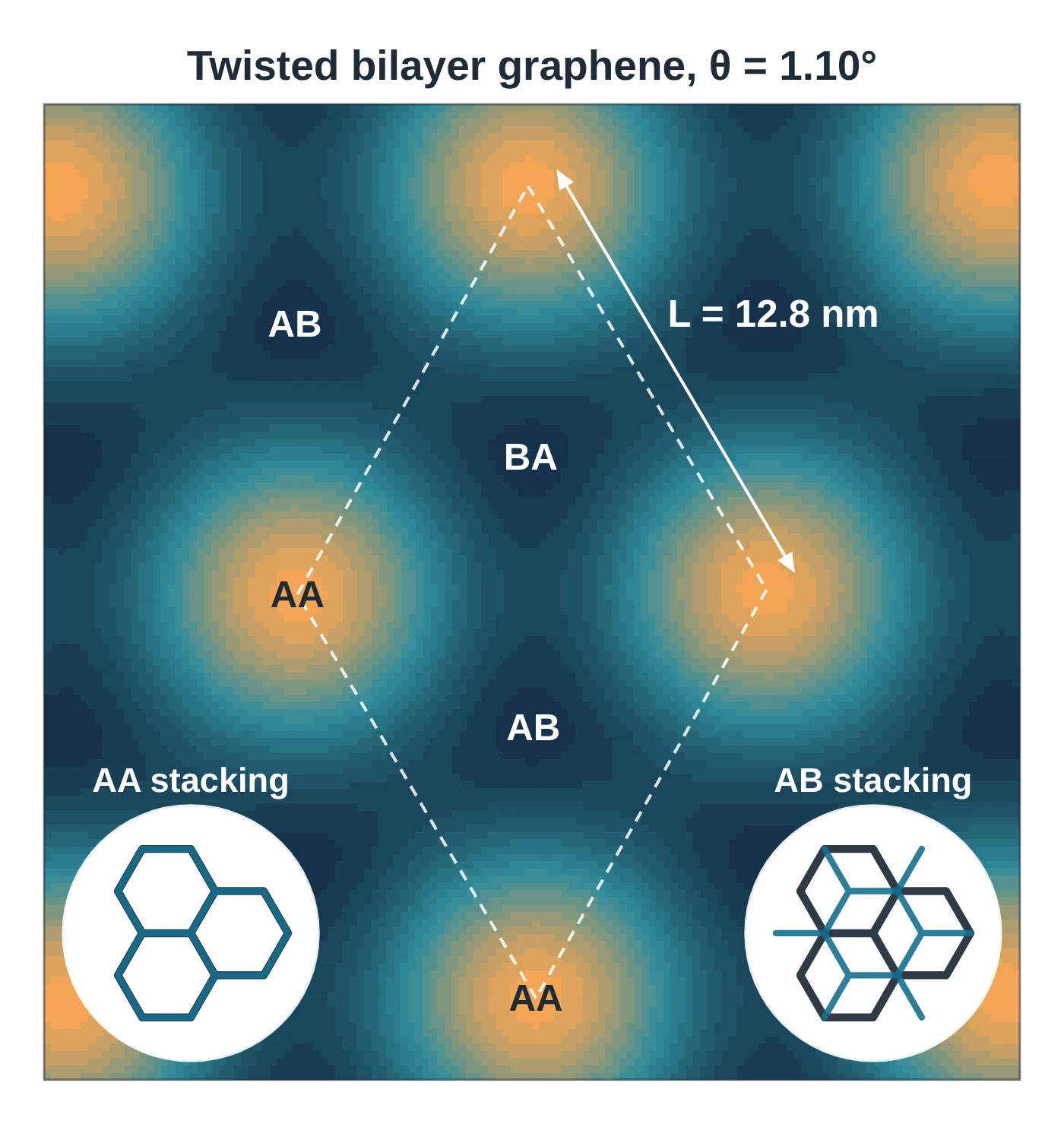
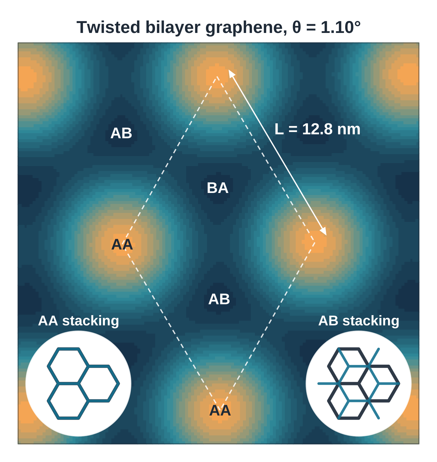
Twisted bilayer graphene (TBG) is two sheets of graphene stacked with one turned by a small angle θ, so that their honeycombs form a moiré pattern of AA, AB and BA stacking regions repeating every L = a / (2 sin(θ/2)), about 12.8 nm at 1.1°. Bistritzer and MacDonald predicted in PNAS in 2011 that at a set of “magic” angles the electrons’ velocity vanishes and the lowest bands become flat; in 2018 Cao, Jarillo-Herrero and co-workers found that bilayers twisted to about 1.1°, the first magic angle, show correlated insulating states and superconductivity up to 1.7 K (Nature 556, 43 and 80).
Last updated
Twisted bilayer graphene at a glance
| Formula | C: two graphene layers, one turned by a twist angle θ |
|---|---|
| Moiré period | L = a / (2 sin(θ/2)) with a = 2.46 Å: about 12.8 nm at 1.1°, 2.8 nm at 5° (calculated) |
| Atoms per moiré cell | About 11,000 at 1.1° (calculated as 4(L/a)²) |
| Stacking regions | AA (atoms on atoms), AB and BA (Bernal) regions alternate across the moiré cell |
| Layer spacing | About 0.335 nm, as in graphite (Sun et al. 2017) |
| Magic angles | A discrete set of twist angles at which the Dirac velocity vanishes and the lowest moiré band flattens (Bistritzer & MacDonald 2011) |
| First magic angle | About 1.1° (Cao et al. 2018, superconductivity) |
| Correlated insulator | Insulating states at half-filling of the flat bands, consistent with Mott-like insulators (Cao et al. 2018, correlated insulator) |
| Superconductivity | Zero-resistance states with a critical temperature up to 1.7 K when doped away from the insulating states (Cao et al. 2018) |
| Phase diagram | Dome-shaped superconducting regions, similar to those of the cuprates (Cao et al. 2018) |
| How it is made | Stacking exfoliated layers with controlled rotation, twist angles controlled below 1° (Kim et al. 2016; Kim et al. 2017) |
| Predicted | Bistritzer & MacDonald, PNAS 108, 12233 (2011) |
| First magic-angle devices | Cao et al., Nature 556, 43 and 556, 80 (2018) |
Twisted bilayer graphene structure diagram

Twisted bilayer graphene structure drawing (high-resolution SVG)
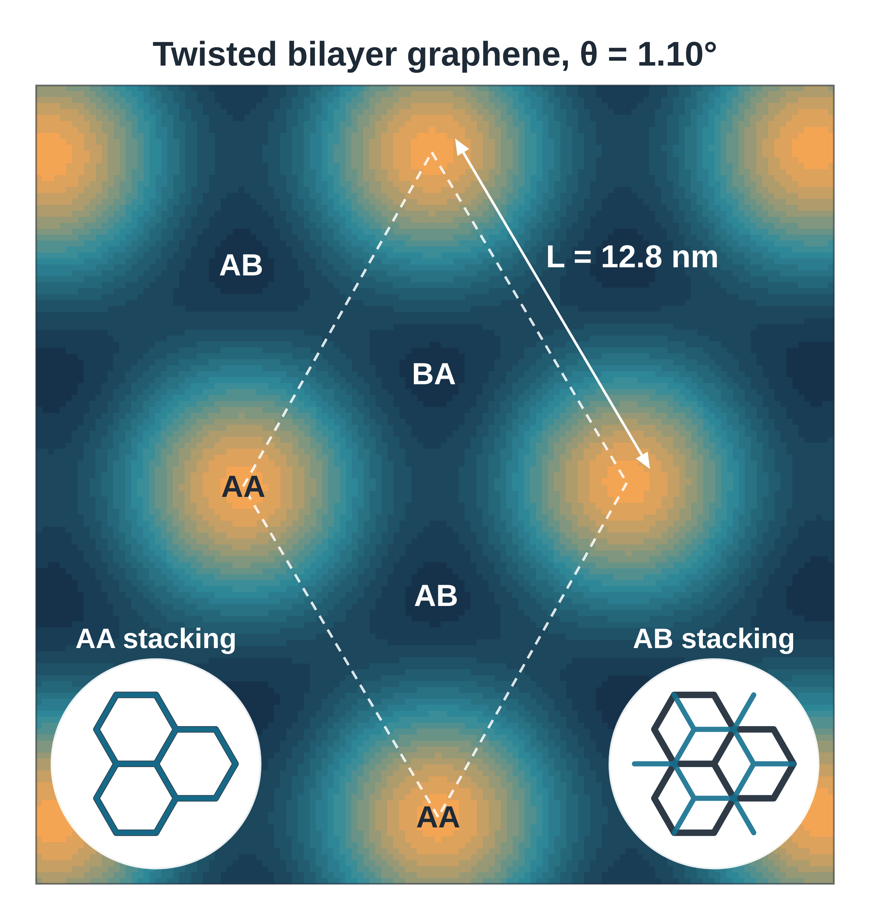
Twisted bilayer graphene in 3D (interactive)
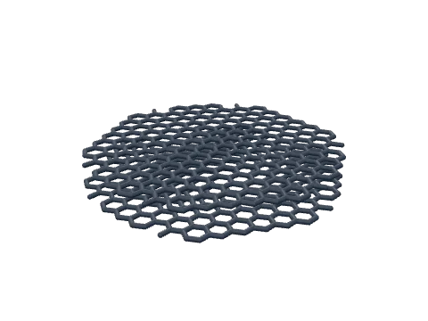
Loading the 3D model…
Twisted bilayer graphene structure explained
Lay one graphene sheet on another and turn it by a small angle θ. Where the two honeycombs line up atom on atom the stacking is AA; a little further on, half the atoms of the top layer sit over hexagon centres of the bottom one, which is the AB (Bernal) stacking of graphite, and then BA. These regions repeat in a triangular moiré pattern with period
L = a / (2 sin(θ/2)), where a = 2.46 Å is graphene’s lattice constant.
The smaller the angle, the larger the moiré: about 2.8 nm at 5° and about 12.8 nm at 1.1°, where one moiré cell holds roughly 11,000 carbon atoms (calculated). The layers stay about 0.335 nm apart, as in graphite (Sun et al. 2017). A similar moiré forms between graphene and hexagonal boron nitride even when they are aligned, because hBN’s lattice constant (2.504 Å) is 1.8 % larger than graphene’s (2.460 Å), giving a period of about 14 nm (Liu et al. 2022; Yankowitz et al. 2012).
The magic angle
Each graphene layer has Dirac cones. In a twisted bilayer, electrons hop between the layers, and the moiré periodicity folds the bands into moiré Bloch bands. Bistritzer and MacDonald (2011) showed in a continuum model that as the twist angle is reduced the layers become more strongly coupled and the Dirac velocity crosses zero several times: at a discrete set of magic angles the velocity vanishes, the lowest moiré band flattens and the density of states at the Dirac point is strongly enhanced.
Cao et al. (2018) confirmed experimentally that near the first magic angle, about 1.1°, the bands near zero Fermi energy become flat and show insulating states at half-filling that are not expected without correlations between electrons, consistent with Mott-like insulators.
How twisted bilayer graphene is made
- Exfoliate. Graphene and hBN flakes are peeled from crystals onto substrates.
- Tear and stack. A polymer stamp carrying hBN picks up part of a graphene flake, tearing it; the substrate is turned by the chosen angle and the rest of the same flake is picked up, so both layers have the same crystal orientation before the twist. Successive transfers with accurate rotational alignment (Kim et al. 2016) gave bilayers with twist angles controlled below 1° (Kim et al. 2017); in hBN-assisted tear-and-stack the angle is fixed when the stack is assembled (Varma Sangani et al. 2020).
- Gate. Contacts and a gate are added, so electrostatic doping tunes the carrier density and therefore the filling of the flat bands (Cao et al. 2018).
Key properties of magic-angle graphene
- Flat bands near zero Fermi energy at twist angles of about 1.1° (Cao et al. 2018).
- Correlated insulators at half-filling of the flat bands, consistent with Mott-like insulator states of electrons localised in the moiré superlattice (Cao et al. 2018, correlated insulator).
- Superconductivity. Doping away from the insulating states gives zero-resistance states with critical temperatures up to 1.7 K; the temperature–density phase diagram has dome-shaped superconducting regions similar to those of the cuprates (Cao et al. 2018).
- Strong pairing. Given its small Fermi surface, its critical temperature puts TBG among the superconductors with the strongest pairing between electrons (Cao et al. 2018).
- Tunable. The filling is set by a gate and the bandwidth by the twist angle (Cao et al. 2018, correlated insulator).
Why twisted bilayer graphene matters
Twisted bilayer graphene is a purely carbon-based, precisely tunable two-dimensional superconductor (Cao et al. 2018). Correlated insulators and superconductivity appear in the same device as a gate changes the filling, and the twist angle is a control knob that conventional heterostructures do not have (Cao et al. 2018, correlated insulator). That makes it a model system for strongly correlated electrons and for questions about high-temperature superconductors.
It also turned the twist angle into a design parameter for all van der Waals heterostructures (Geim & Grigorieva 2013): aligned graphene on hBN, for example, gives a moiré superlattice in which a Hofstadter butterfly was observed (Hunt et al. 2013).
Uses and research areas
- Correlated electron physics. Mott-like insulators and unconventional superconductivity in one tunable device (Cao et al. 2018).
- Moiré superlattices. Graphene on hBN, with superlattice Dirac points (Yankowitz et al. 2012) and massive Dirac fermions (Hunt et al. 2013).
- Device assembly. Methods to set and hold the twist angle (Kim et al. 2016; Varma Sangani et al. 2020).
- Imaging. Scanning tunnelling microscopy shows the moiré directly (Yankowitz et al. 2012).
How to draw twisted bilayer graphene
For a paper, slide or poster, show the two honeycombs with one turned, the resulting moiré with its AA, AB and BA regions and the period L, and, for the physics, the flat bands at the magic angle. The moiré figure above shows tear-and-stack assembly, the pattern, the two layers in 3D, the magic angle and graphene on hBN, and opens as an editable LabCanvas figure. The structure drawing is a high-resolution SVG of the figure editor’s magic-angle stacking map, in which you can change the twist or switch to the atoms of both layers. The 3D model opens in the LabCanvas 3D Studio, where you can change the twist angle and export a high-resolution image. A twisted bilayer has no ordinary crystal file, so there is no crystal structure drawing on this page.
Twisted bilayer graphene compared with other 2D materials
| Material | Composition | Layer structure | Electronic character | Made by | Key paper |
|---|---|---|---|---|---|
| Twisted bilayer graphene | C | Two graphene layers turned by θ; moiré period 12.8 nm at 1.1° | Flat bands at the magic angle; correlated insulator and superconductor (up to 1.7 K) | Tear and stack of exfoliated graphene | Cao et al., Nature 2018 |
| Graphene | C | Flat honeycomb, one atom thick, a = 2.46 Å | Zero-gap semimetal (Dirac cones) | Tape, CVD on Cu, SiC, liquid exfoliation | Novoselov et al., Science 2004 |
| Graphene oxide | C, O, H (no fixed formula) | Honeycomb carrying epoxides and hydroxyls; carboxyls at the edges | Only about a quarter of the carbon sp²; reduced to rGO to conduct | Oxidising graphite (Hummers), then exfoliation in water | Hummers & Offeman, JACS 1958 |
| h-BN | BN | Honeycomb of alternating B and N, a = 2.504 Å | Wide direct-gap insulator (luminescence at 215 nm) | Exfoliated from crystals | Dean et al., Nat. Nanotechnol. 2010 |
| MoS₂ | MoS₂ | S–Mo–S sandwich, three atoms thick | Semiconductor; 1.8 eV direct gap as a monolayer | Exfoliation, CVD | Mak et al., PRL 2010; Radisavljevic et al. 2011 |
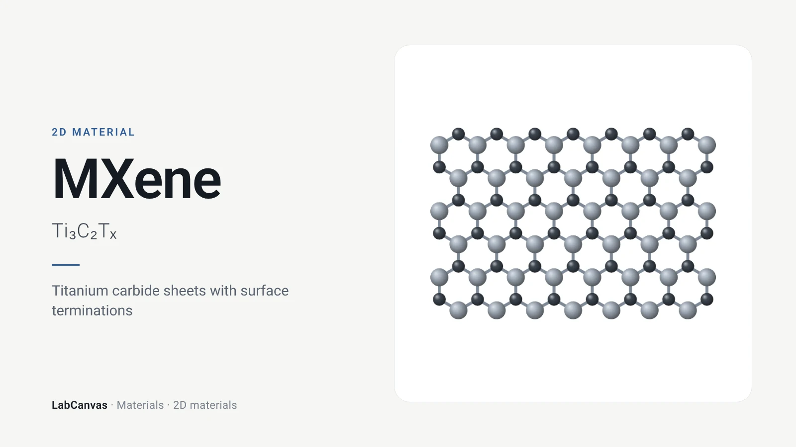
| MXene (Ti₃C₂Tₓ) | Ti₃C₂ with –O, –OH, –F | Ti–C–Ti–C–Ti layers with terminated faces | — | Etching Al out of the MAX phase Ti₃AlC₂ | Naguib et al., Adv. Mater. 2011 |
Related materials
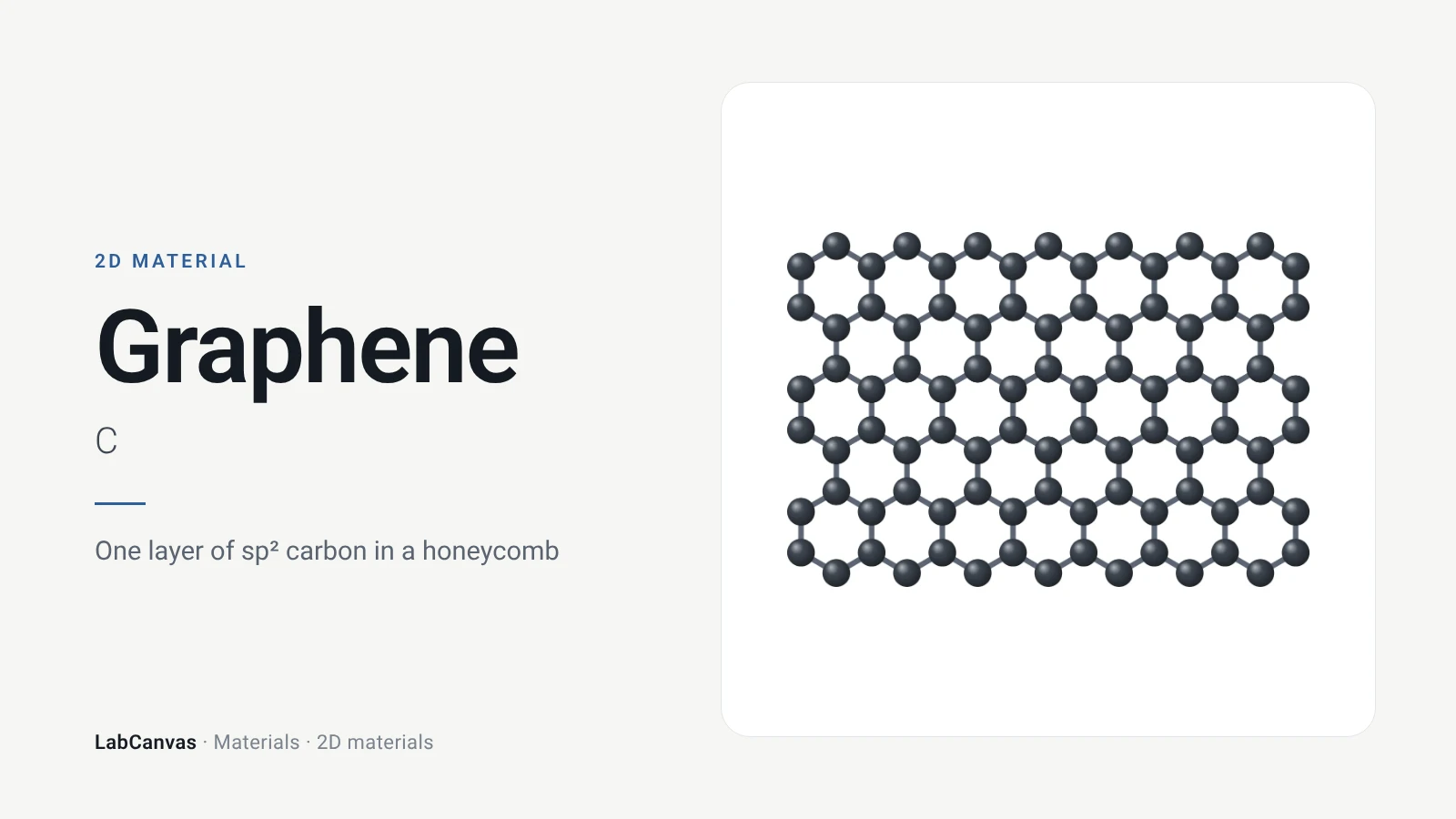
Graphene
Graphene structure explained: the one-atom-thick honeycomb of sp² carbon, its Dirac bands, strength and conductivity, how it is made and used. Cited facts.
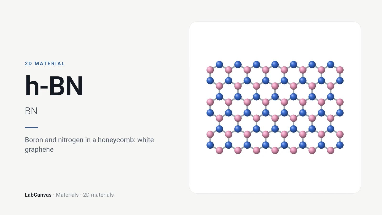
Hexagonal boron nitride (h-BN)
Hexagonal boron nitride (h-BN), “white graphene”: its B–N honeycomb structure, ~6 eV band gap, how it is made and why 2D devices sit on it. Editable figures.
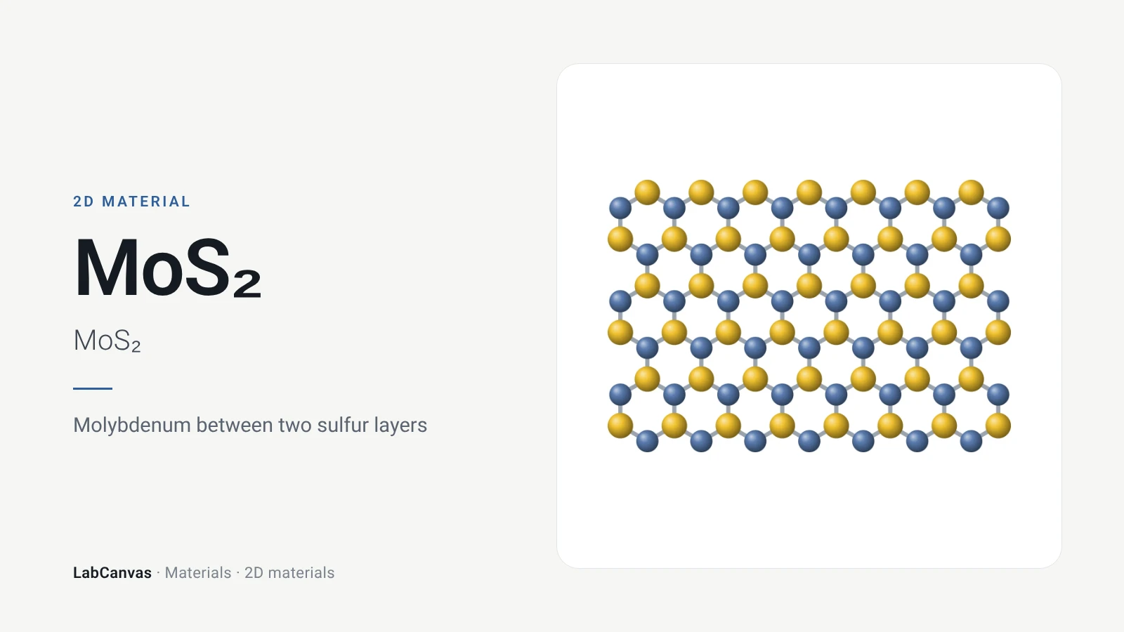
MoS₂ (molybdenum disulfide)
MoS₂ structure and band gap: the S–Mo–S layer, 2H and 1T phases, the 1.8 eV direct gap of monolayer MoS₂, transistors and HER catalysis. Editable figures.
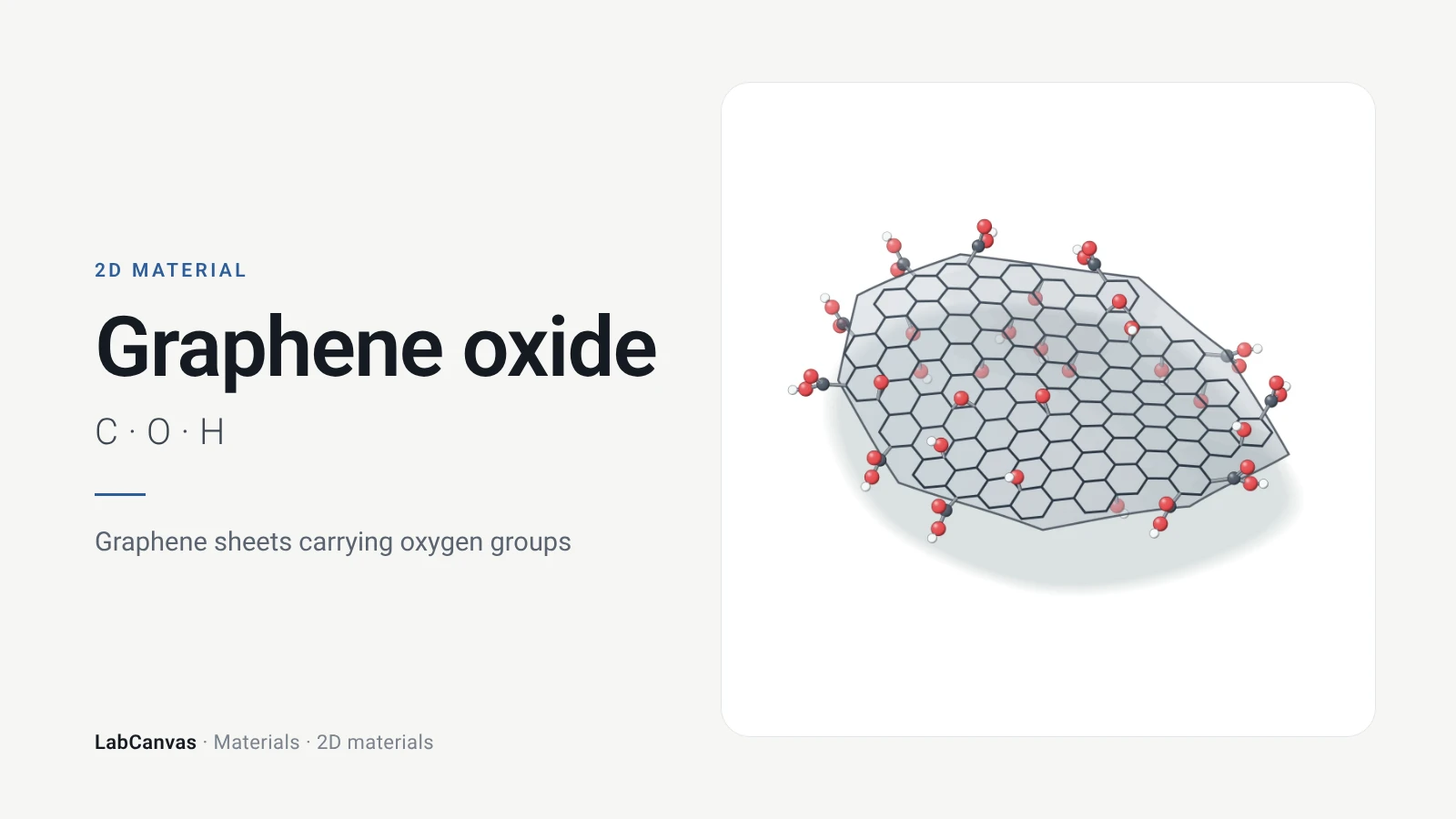
Graphene oxide
Graphene oxide structure explained: graphene with epoxide, hydroxyl and carboxyl groups, made by the Hummers method and reduced to rGO. Cited facts, figures.
MXene (Ti₃C₂Tₓ)
MXene Ti₃C₂Tₓ explained: 2D titanium carbide etched from the MAX phase Ti₃AlC₂, its surface terminations, synthesis, conductivity and uses. Editable figures.
COF-5
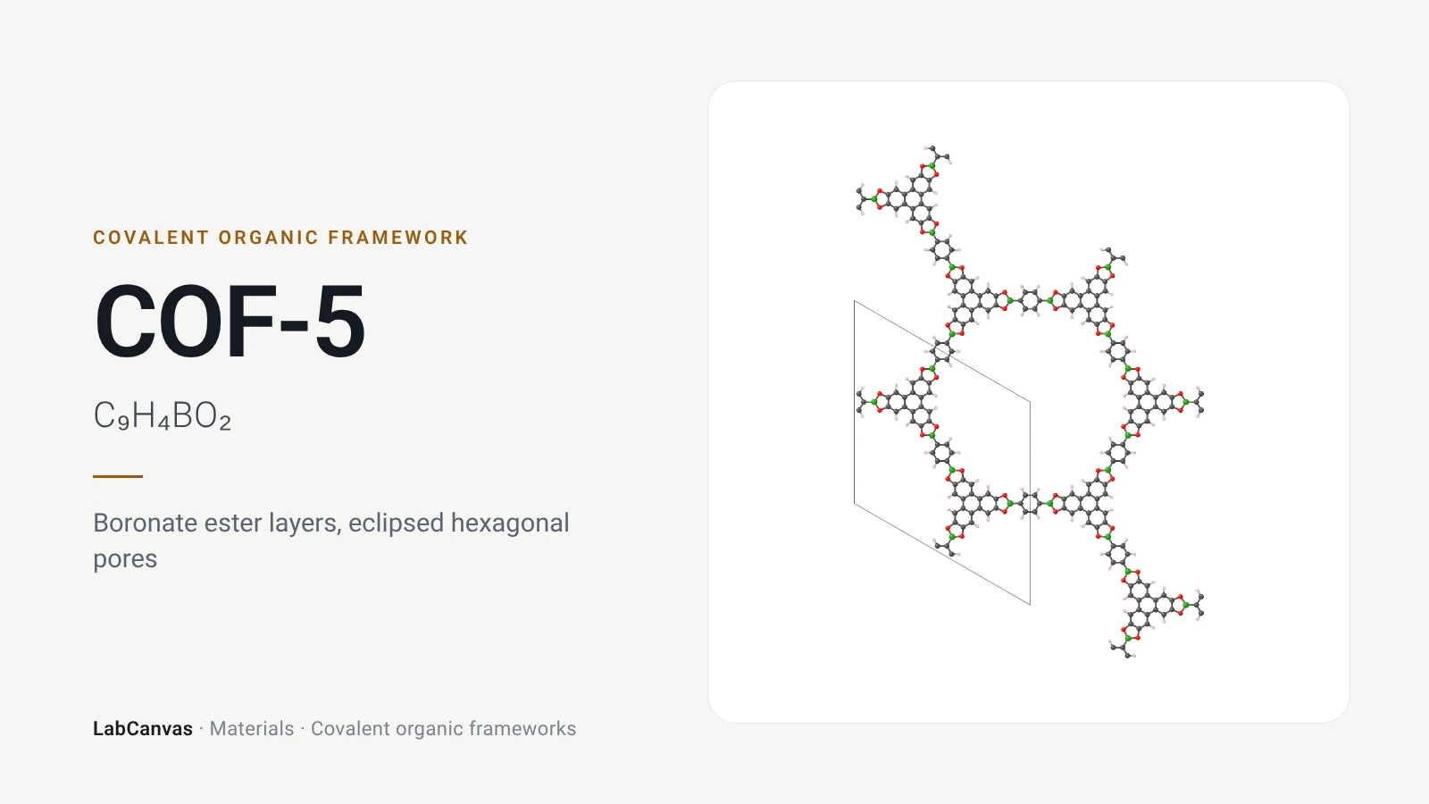
COF-5, the boronate ester COF from HHTP and BDBA: eclipsed layers, 27 Å channels, 1,590 m² g⁻¹, synthesis and stability, with 2D and 3D figures to edit.
More on LabCanvas
- Twisted bilayers and moiré superlattices: Editable figure template
- More figure templates in this category: Ready-made, cited figures to edit
- Crystal structure figure software compared: VESTA, Mercury, CrystalMaker, Avogadro and LabCanvas
- XRD Scherrer crystallite size calculator: Free tool
- Molar mass calculator: Free tool
- Journal figure size guide: Column widths and resolutions for 38 journals
- 3D models gallery: Turn MOFs, COFs and more in 3D
Frequently asked questions
What is twisted bilayer graphene?
Two layers of graphene stacked with one rotated by a small angle relative to the other. The mismatch makes a moiré pattern, a superlattice much larger than the atomic lattice, which reshapes the electronic bands.
What is the magic angle in twisted bilayer graphene?
About 1.1°, the first of a set of “magic” twist angles at which the Dirac velocity vanishes and the lowest moiré bands become flat (predicted by Bistritzer & MacDonald, PNAS 2011; measured by Cao et al., Nature 2018).
Why is the magic angle important?
At the magic angle the bands near zero energy become flat, and correlations between electrons take over: magic-angle graphene shows correlated insulating states at half-filling and, when doped, superconductivity up to 1.7 K (Cao et al., Nature 2018).
Is twisted bilayer graphene a superconductor?
Near the magic angle, yes: Cao et al. (Nature 2018) found zero-resistance states with critical temperatures up to 1.7 K when the bilayer is doped away from its correlated insulating states.
What is a moiré pattern in graphene?
The interference pattern of two overlaid lattices. In a twisted bilayer, regions where the atoms sit on top of each other (AA) alternate with Bernal-stacked regions (AB and BA) with a period L = a / (2 sin(θ/2)), about 12.8 nm at 1.1° for a = 2.46 Å.
How is twisted bilayer graphene made?
Usually by tear and stack: a stamp carrying hBN picks up half of an exfoliated graphene flake, the substrate is rotated by the target angle and the other half is picked up on top. Rotational alignment methods have controlled twist angles below 1° (Kim et al., PNAS 2017).
What is twistronics?
An informal name for using the twist angle between stacked 2D layers to set their electronic properties, as in magic-angle twisted bilayer graphene.
How is twisted bilayer graphene different from AB bilayer graphene?
AB (Bernal) bilayer graphene has every second layer shifted, the stacking of graphite, and has no moiré. A twisted bilayer contains AA, AB and BA regions in a moiré superlattice whose size and bands depend on the twist angle.
How can I draw twisted bilayer graphene for a paper or presentation?
Open the moiré figure on this page in LabCanvas (free), add the magic-angle stacking map from the figure editor’s Library and change the twist, or open the 3D model in the LabCanvas 3D Studio and export a render.
References
- R. Bistritzer, A. H. MacDonald. Moiré bands in twisted double-layer graphene. Proc. Natl. Acad. Sci. USA 2011, 108, 12233–12237. doi:10.1073/pnas.1108174108
- Y. Cao, V. Fatemi, S. Fang, K. Watanabe, T. Taniguchi, E. Kaxiras, P. Jarillo-Herrero. Unconventional superconductivity in magic-angle graphene superlattices. Nature 2018, 556, 43–50. doi:10.1038/nature26160
- Y. Cao et al.. Correlated insulator behaviour at half-filling in magic-angle graphene superlattices. Nature 2018, 556, 80–84. doi:10.1038/nature26154
- K. Kim et al.. van der Waals heterostructures with high accuracy rotational alignment. Nano Lett. 2016, 16, 1989. doi:10.1021/acs.nanolett.5b05263
- K. Kim et al.. Tunable moiré bands and strong correlations in small-twist-angle bilayer graphene. Proc. Natl. Acad. Sci. USA 2017, 114, 3364. doi:10.1073/pnas.1620140114
- Varma Sangani et al.. Facile deterministic cutting of 2D materials for twistronics using a tapered fibre scalpel. Nanotechnology 2020, 31, 32LT02. doi:10.1088/1361-6528/ab8b93
- M. Yankowitz et al.. Emergence of superlattice Dirac points in graphene on hexagonal boron nitride. Nat. Phys. 2012, 8, 382. doi:10.1038/nphys2272
- B. Hunt et al.. Massive Dirac fermions and Hofstadter butterfly in a van der Waals heterostructure. Science 2013, 340, 1427. doi:10.1126/science.1237240
- X. Liu et al.. Influence of hexagonal boron nitride on electronic structure of graphene. Molecules 2022, 27, 3740. doi:10.3390/molecules27123740
- Y. Sun et al.. Comparison of reduction products from graphite oxide and graphene oxide for anode applications in lithium-ion batteries and sodium-ion batteries. Nanoscale 2017, 9, 2585. doi:10.1039/c6nr07650e
- A. H. Castro Neto et al.. The electronic properties of graphene. Rev. Mod. Phys. 2009, 81, 109. doi:10.1103/RevModPhys.81.109
- A. K. Geim, I. V. Grigorieva. Van der Waals heterostructures. Nature 2013, 499, 419. doi:10.1038/nature12385
- K. S. Novoselov et al.. Electric field effect in atomically thin carbon films. Science 2004, 306, 666–669. doi:10.1126/science.1102896
Draw Twisted bilayer graphene for your paper or slides
LabCanvas is a browser workspace for scientific figures: framework clusters, linkers and nets, crystal structures in 2D and 3D, graphs and posters, all editable.
Edit the Twisted bilayer graphene figure