Graphene: structure, properties and synthesis
Graphene is a single layer of carbon atoms, one atom thick, bonded in a flat honeycomb lattice: each sp² carbon joined to three neighbours 1.42 Å away, two atoms per hexagonal cell with a = 2.46 Å. Stacked, graphene sheets make graphite. It was first isolated by peeling graphite with adhesive tape and measured by Novoselov, Geim and co-workers in Science in 2004, who found a two-dimensional semimetal, stable in air, with room-temperature mobilities of about 10,000 cm² V⁻¹ s⁻¹.
Last updated
Graphene at a glance
| Formula | C: a single layer of sp² carbon (Novoselov et al. 2004) |
|---|---|
| Lattice | Hexagonal honeycomb, two carbon atoms (A and B sublattices) per unit cell (Castro Neto et al. 2009) |
| C–C bond length | 1.42 Å (Castro Neto et al. 2009) |
| Lattice constant | a = 2.46 Å, that is √3 × 1.42 Å (Castro Neto et al. 2009) |
| Atom density | 3.82 × 10¹⁵ carbon atoms per cm², 0.76 mg m⁻² (calculated from a = 2.46 Å) |
| Specific surface area | About 2,630 m² g⁻¹ counting both faces (calculated from the areal mass) |
| Layer spacing in graphite | 0.335 nm (Sun et al. 2017) |
| Electronic structure | Zero-gap semimetal: the π and π* bands meet at the K points in Dirac cones (Castro Neto et al. 2009; Novoselov et al. 2004) |
| Carrier speed | About 10⁶ m s⁻¹, independent of energy near the Dirac point (Castro Neto et al. 2009) |
| Mobility | About 10,000 cm² V⁻¹ s⁻¹ at room temperature, carriers up to 10¹³ cm⁻² by gating (Novoselov et al. 2004); almost ten times better on h-BN than on SiO₂ (Dean et al. 2010) |
| Stiffness and strength | Young’s modulus 1.0 TPa, intrinsic strength 130 GPa (2D: 340 and 42 N m⁻¹) (Lee et al. 2008) |
| Thermal conductivity | (4.84–5.30) × 10³ W m⁻¹ K⁻¹ for suspended single layers at room temperature (Balandin et al. 2008) |
| Optical absorption | 2.3 % of white light per layer (πα) (Nair et al. 2008) |
| Gas permeability | A monolayer membrane is impermeable to standard gases, including helium (Bunch et al. 2008) |
| First isolated | Novoselov, Geim et al., Science 306, 666 (2004) |
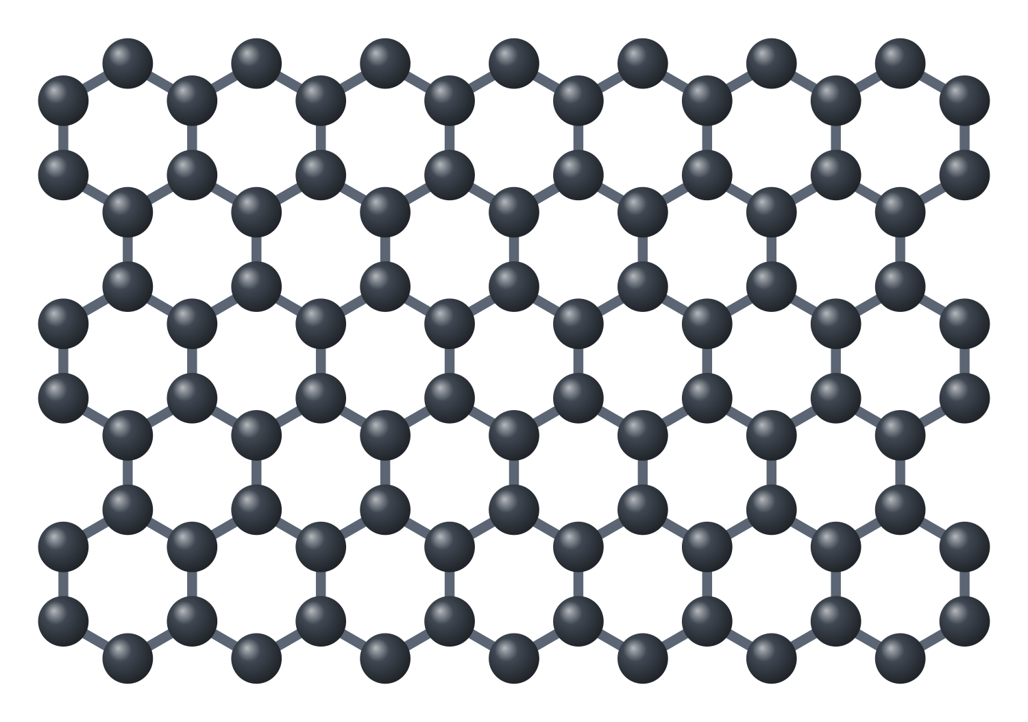
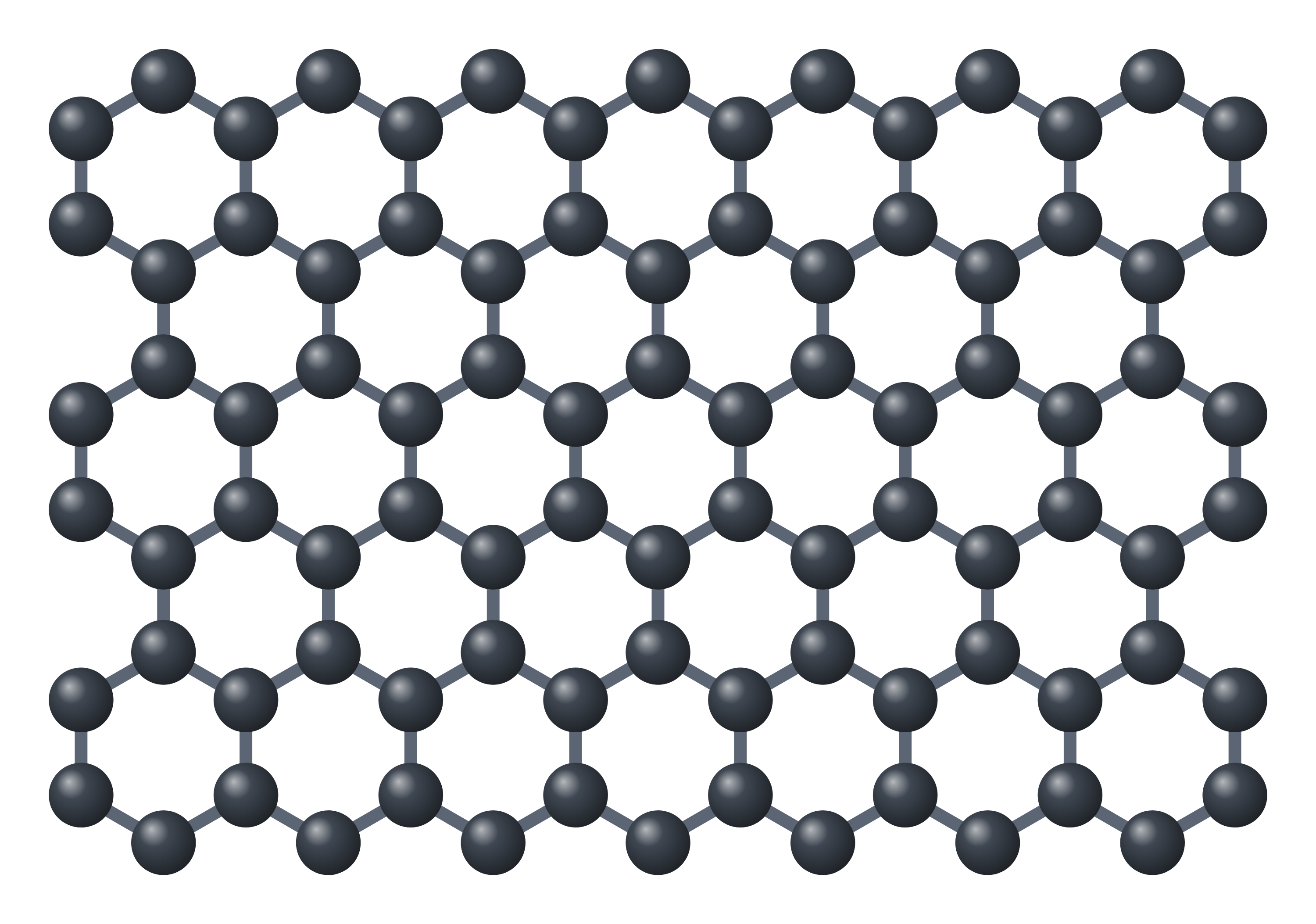
Graphene structure diagram

Graphene crystal structure (high-resolution SVG)
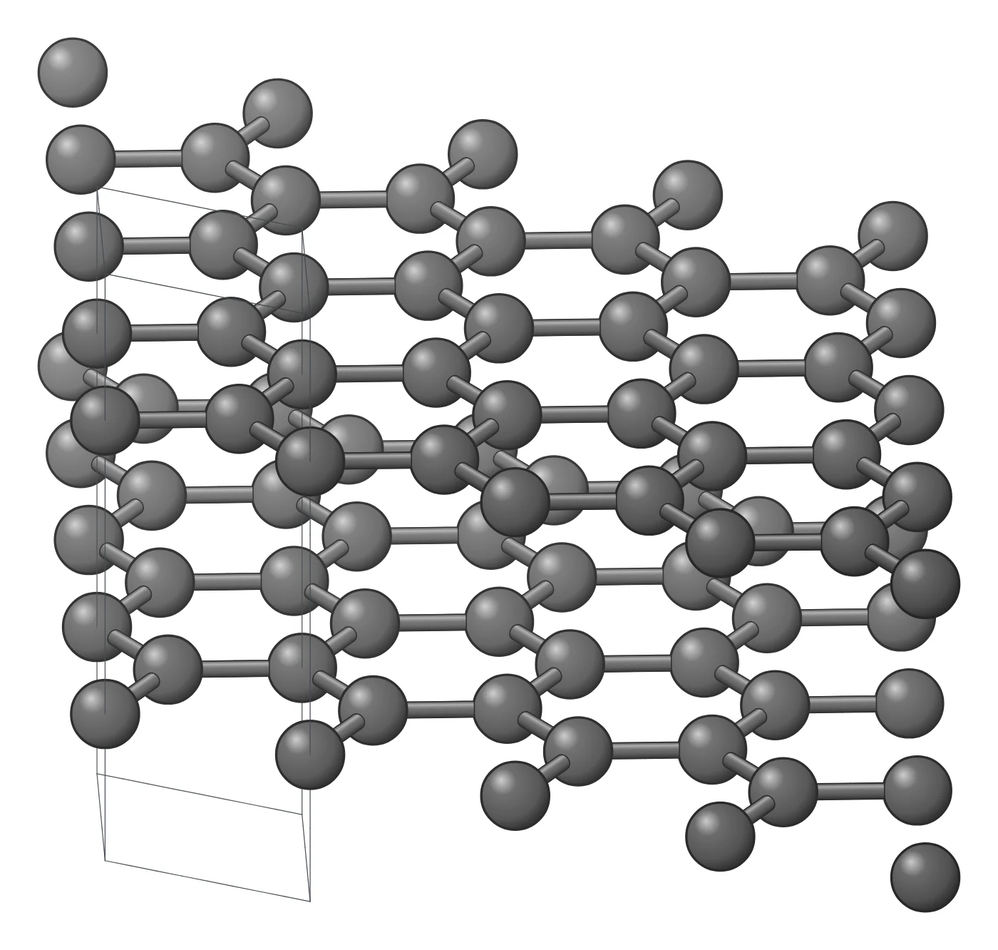
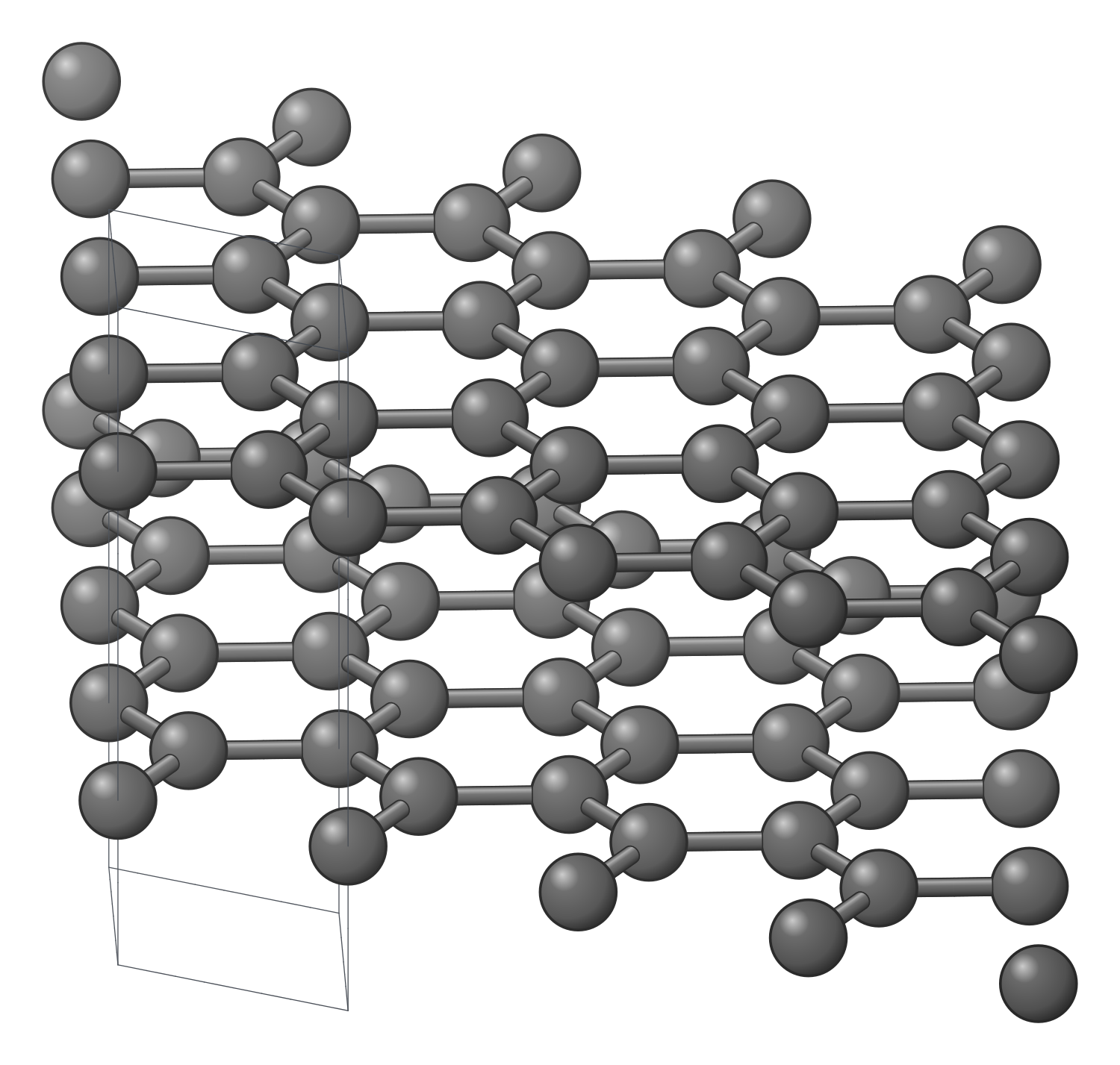
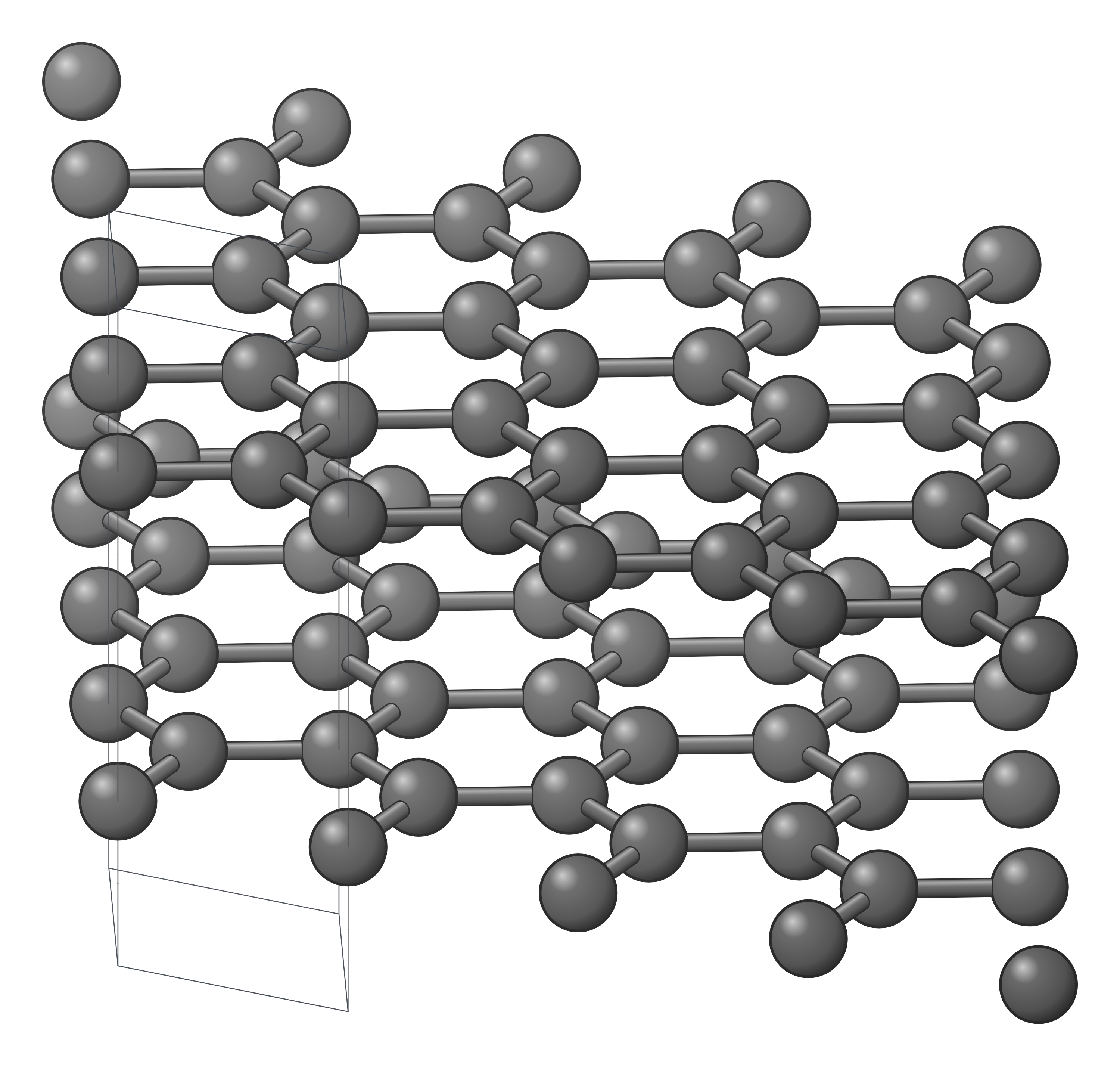
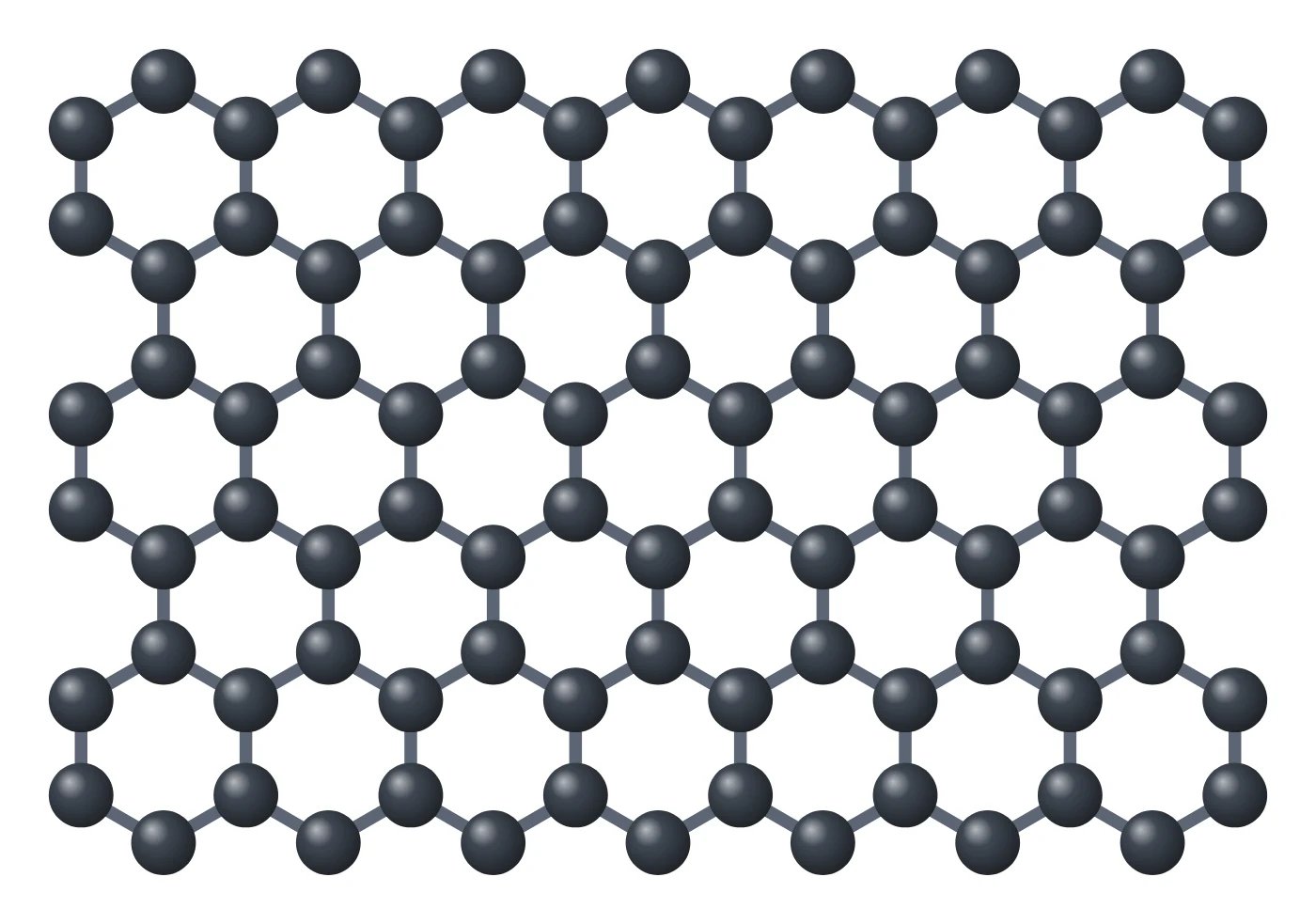
Graphene structure drawing (high-resolution SVG)
Graphene in 3D (interactive)
Loading the 3D model…
More Graphene figures


Graphene structure explained
Graphene is carbon in its simplest two-dimensional form. Each carbon atom is sp² hybridised: three of its electrons form σ bonds to three neighbours in the plane, 120° apart and 1.42 Å long, and the fourth sits in a p orbital perpendicular to the sheet. The p orbitals of all the atoms overlap into the π system that gives graphene its electronic properties (Castro Neto et al. 2009).
The atoms form a honeycomb. It is not a Bravais lattice on its own: it is a hexagonal lattice with a two-atom basis, the A and B sublattices. The cell vectors a₁ and a₂ are 2.46 Å long (√3 × 1.42 Å) and 60° apart, so the cell holds two atoms in 5.24 Ų, which works out at 3.82 × 10¹⁵ atoms per cm² and 0.76 mg per m² (calculated).
Stack graphene sheets on top of one another, every second sheet shifted so that half its atoms sit over hexagon centres, and you have graphite (AB or Bernal stacking), with the layers 0.335 nm apart (Sun et al. 2017) and held only by van der Waals forces. That weak bonding between layers is why a single sheet can be peeled off.
How graphene is made
- Mechanical exfoliation. Graphite is peeled apart with adhesive tape; this gave the first few-atom-thick crystals, of remarkably high quality (Novoselov et al. 2004). It is still the route for the best research devices.
- Liquid-phase and shear exfoliation. Graphite is exfoliated in a solvent whose surface energy matches graphene’s, such as NMP, giving about 1 wt % monolayers (Hernandez et al. 2008); high-shear mixing scales this from hundreds of millilitres to hundreds of litres (Paton et al. 2014).
- Graphene oxide and reduction. Graphite is oxidised (Hummers & Offeman 1958), split into graphene oxide in water and reduced; easy to scale, but the product stays defective (Luong et al. 2020). See the graphene oxide page.
- Chemical vapour deposition (CVD). Methane on copper foil gives centimetre-scale films that are mostly one layer, less than 5 % of the area thicker (Li et al. 2009); roll-to-roll transfer makes 30-inch films (Bae et al. 2010).
- Epitaxy on SiC. Heating silicon carbide in about 1 bar of argon drives off silicon from the Si face and leaves graphene films (Emtsev et al. 2009).
- Flash Joule heating. A current pulse turns coal, carbon black or plastic waste into gram-scale turbostratic graphene in less than a second (Luong et al. 2020).
Key properties of graphene
- Electronic. The π and π* bands touch at the corners of the Brillouin zone (the K points), where they are linear in momentum: the Dirac cones. Graphene is therefore a zero-gap semimetal whose carriers move at about 10⁶ m s⁻¹ as if they had no mass (Castro Neto et al. 2009). A gate tunes the carriers continuously from electrons to holes, up to 10¹³ cm⁻² (Novoselov et al. 2004).
- Quantum Hall effect. In a magnetic field graphene shows a half-integer quantum Hall effect, σxy = ±4(N + ½)e²/h, a direct signature of its Dirac carriers (Novoselov et al. 2005; Zhang et al. 2005).
- Mobility. About 10,000 cm² V⁻¹ s⁻¹ at room temperature on SiO₂ in the first devices (Novoselov et al. 2004); on atomically flat h-BN, mobility and carrier uniformity are almost an order of magnitude better (Dean et al. 2010).
- Mechanical. Nanoindentation of suspended sheets gave a Young’s modulus of 1.0 TPa and an intrinsic strength of 130 GPa, “the strongest material ever measured” (Lee et al. 2008).
- Thermal. Suspended single layers conduct heat at (4.84–5.30) × 10³ W m⁻¹ K⁻¹ at room temperature (Balandin et al. 2008).
- Optical. One layer absorbs πα = 2.3 % of white light, a value set by the fine-structure constant (Nair et al. 2008).
- Barrier. A defect-free monolayer is impermeable to standard gases, including helium (Bunch et al. 2008).
Why graphene matters
The 2004 Science paper showed films a few atoms thick that were stable in air, metallic and of high quality, with a strong ambipolar field effect (Novoselov et al. 2004). The following year two groups measured the half-integer quantum Hall effect, confirming that graphene’s carriers behave as massless Dirac fermions (Novoselov et al. 2005; Zhang et al. 2005).
Graphene opened the field of 2D materials. The same peeling and transfer methods gave insulating h-BN, semiconducting MoS₂ and many more, and these layers can be restacked in a chosen order into van der Waals heterostructures (Geim & Grigorieva 2013), including twisted bilayer graphene.
Uses and research areas
- Transparent electrodes. Roll-to-roll CVD films reached about 125 Ω per square at 97.4 % transmittance (Bae et al. 2010).
- Composites. Graphene sheets in polystyrene conduct electricity above about 0.1 vol % (Stankovich et al. 2006).
- Electronics and physics. High-mobility devices on h-BN (Dean et al. 2010), moiré superlattices and twisted bilayers (Cao et al. 2018).
- Thermal management. Its thermal conductivity makes it an excellent material for thermal management (Balandin et al. 2008).
- Membranes and barriers. Impermeable sheets (Bunch et al. 2008) and graphene oxide laminates that sieve ions (Joshi et al. 2014).
- Quality control. Raman spectroscopy counts layers and measures defects without damage (Ferrari et al. 2006); a monolayer at 532 nm has FWHM(2D) ≤ 35 cm⁻¹ and I(2D)/I(G) ≥ 2 (Muñoz-Vargas et al. 2025).
How to draw the graphene structure
For a paper, slide or poster, start from the honeycomb: two atoms per cell, bonds of 1.42 Å, and the cell vectors of 2.46 Å if you want to show the lattice. The Dirac physics figure above adds the Brillouin zone and the Dirac cone, the production figure shows how it is made and the Raman figure how it is checked; each opens as an editable LabCanvas figure. The structure drawing is a high-resolution SVG of the figure editor’s graphene object, which you can tilt, ripple or switch to h-BN, MoS₂ or MXene. The crystal structure drawing shows graphite, the AB stack of graphene sheets, from its crystal file and opens in the figure editor, where you can change the style, the number of cells and the view. The 3D model opens in the LabCanvas 3D Studio, where you can add layers or a twist and export a high-resolution image.
Graphene compared with other 2D materials
| Material | Composition | Layer structure | Electronic character | Made by | Key paper |
|---|---|---|---|---|---|
| Graphene | C | Flat honeycomb, one atom thick, a = 2.46 Å | Zero-gap semimetal (Dirac cones) | Tape, CVD on Cu, SiC, liquid exfoliation | Novoselov et al., Science 2004 |
| Graphene oxide | C, O, H (no fixed formula) | Honeycomb carrying epoxides and hydroxyls; carboxyls at the edges | Only about a quarter of the carbon sp²; reduced to rGO to conduct | Oxidising graphite (Hummers), then exfoliation in water | Hummers & Offeman, JACS 1958 |
| h-BN | BN | Honeycomb of alternating B and N, a = 2.504 Å | Wide direct-gap insulator (luminescence at 215 nm) | Exfoliated from crystals | Dean et al., Nat. Nanotechnol. 2010 |
| MoS₂ | MoS₂ | S–Mo–S sandwich, three atoms thick | Semiconductor; 1.8 eV direct gap as a monolayer | Exfoliation, CVD | Mak et al., PRL 2010; Radisavljevic et al. 2011 |
| MXene (Ti₃C₂Tₓ) | Ti₃C₂ with –O, –OH, –F | Ti–C–Ti–C–Ti layers with terminated faces | — | Etching Al out of the MAX phase Ti₃AlC₂ | Naguib et al., Adv. Mater. 2011 |
Related materials
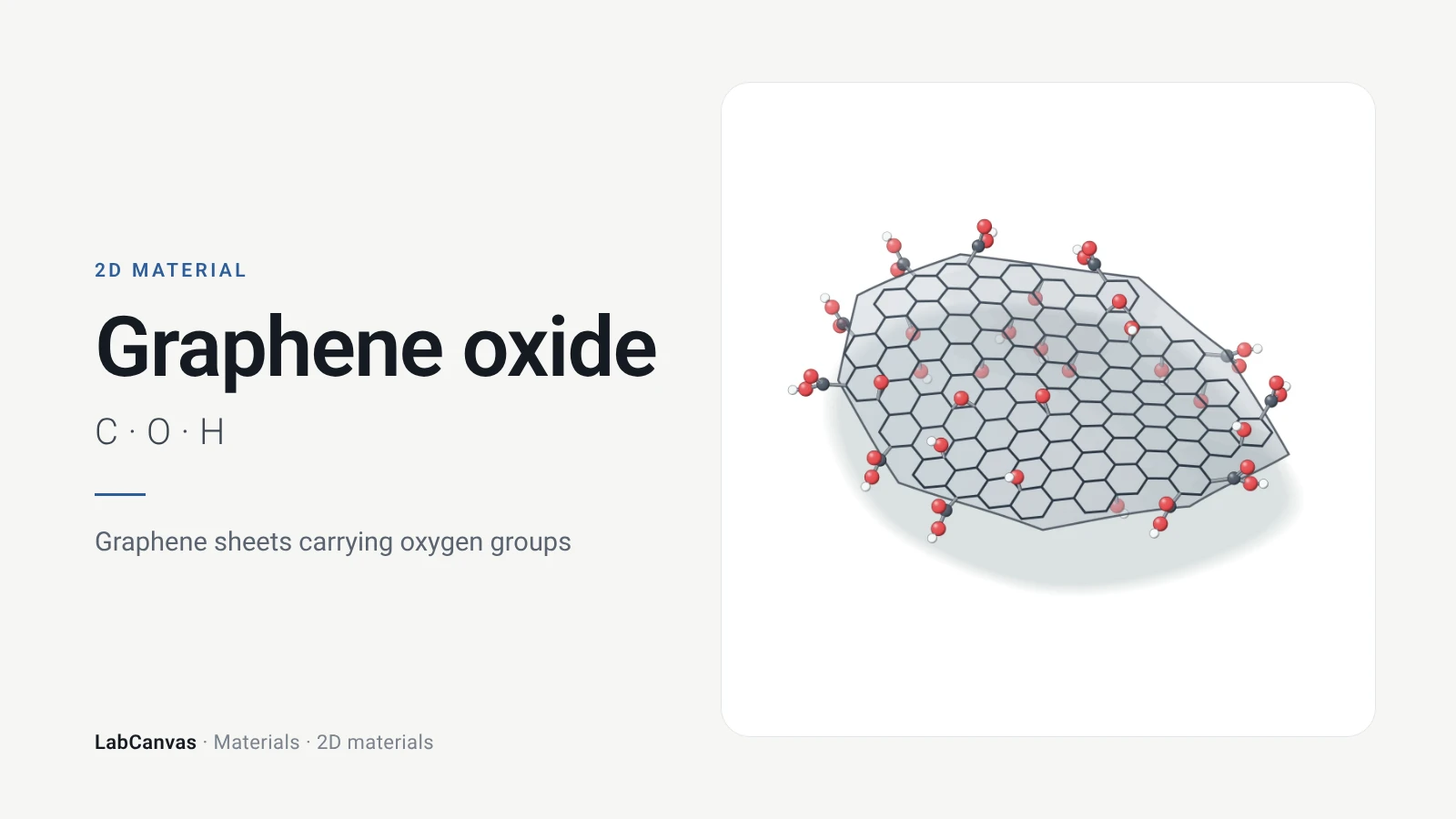
Graphene oxide
Graphene oxide structure explained: graphene with epoxide, hydroxyl and carboxyl groups, made by the Hummers method and reduced to rGO. Cited facts, figures.
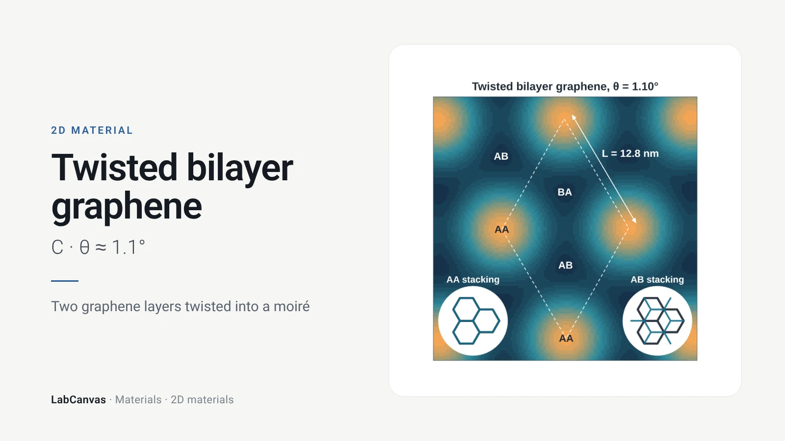
Twisted bilayer graphene
Twisted bilayer graphene explained: two layers turned by a small angle, the moiré, the 1.1° magic angle, flat bands and superconductivity. Cited papers.
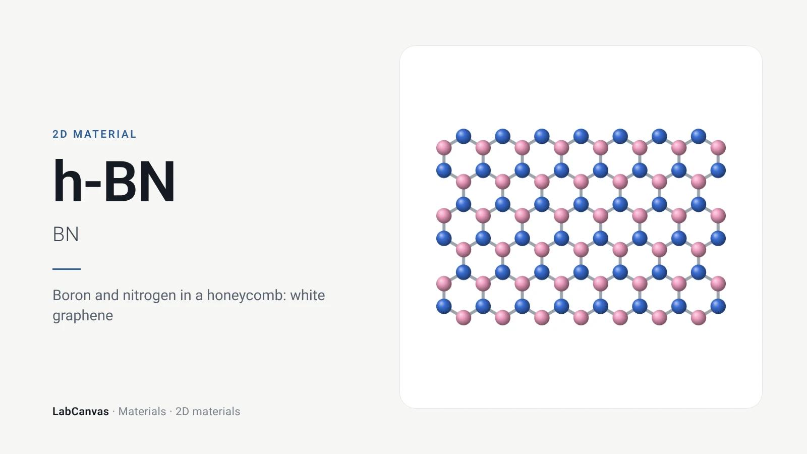
Hexagonal boron nitride (h-BN)
Hexagonal boron nitride (h-BN), “white graphene”: its B–N honeycomb structure, ~6 eV band gap, how it is made and why 2D devices sit on it. Editable figures.
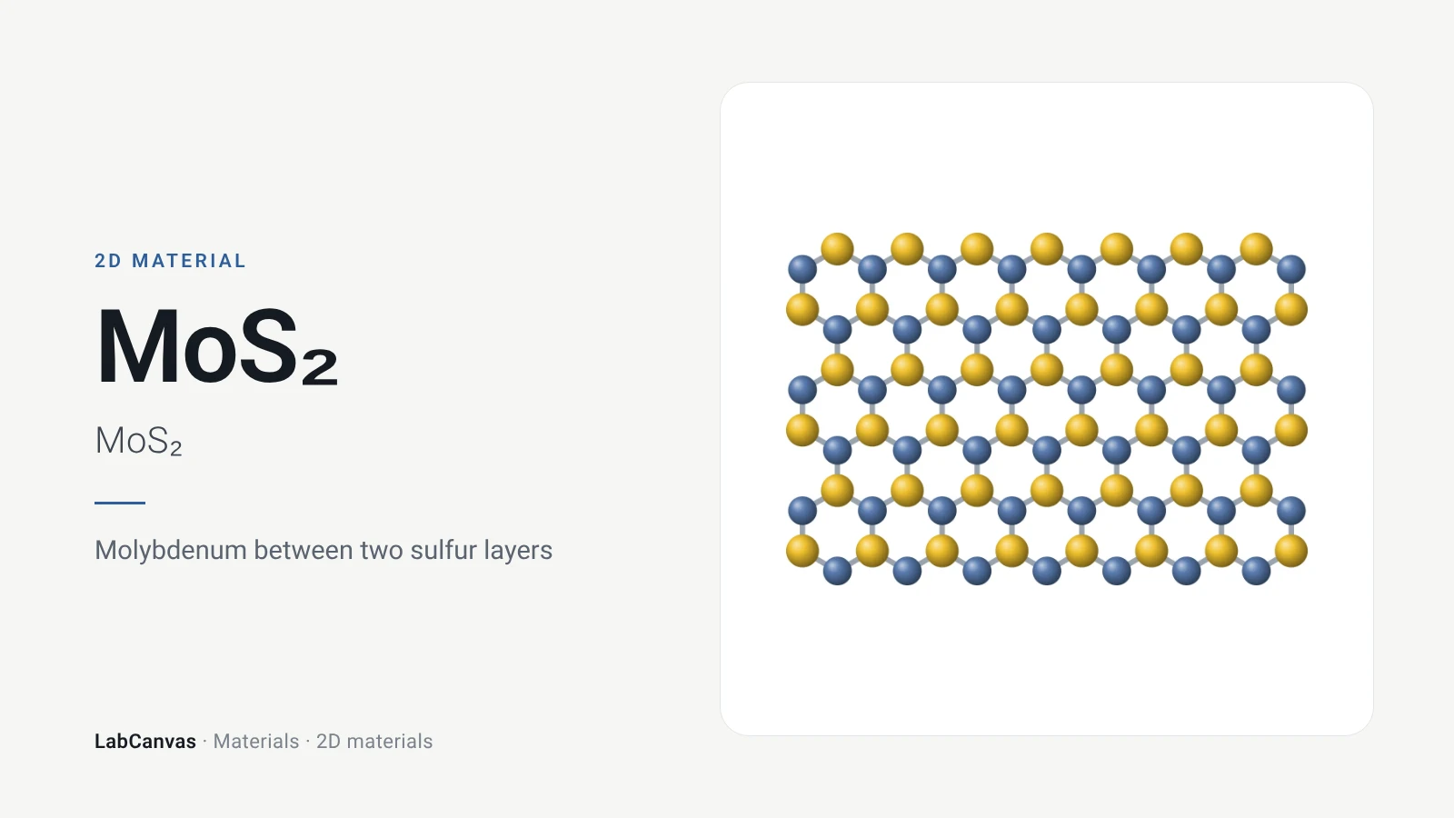
MoS₂ (molybdenum disulfide)
MoS₂ structure and band gap: the S–Mo–S layer, 2H and 1T phases, the 1.8 eV direct gap of monolayer MoS₂, transistors and HER catalysis. Editable figures.
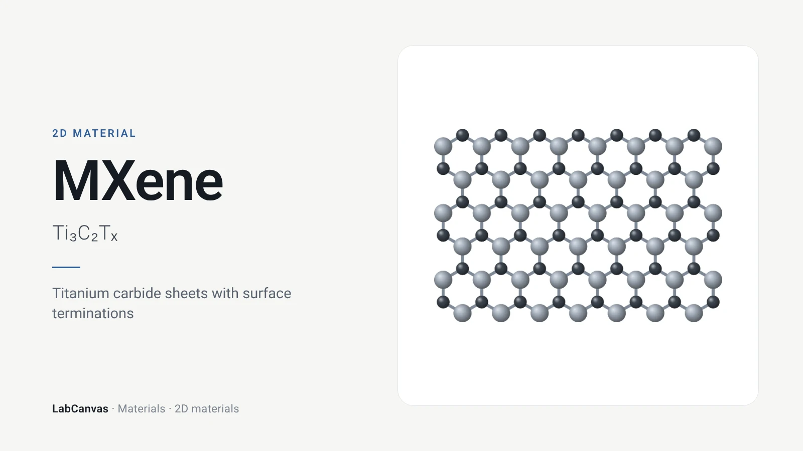
MXene (Ti₃C₂Tₓ)
MXene Ti₃C₂Tₓ explained: 2D titanium carbide etched from the MAX phase Ti₃AlC₂, its surface terminations, synthesis, conductivity and uses. Editable figures.
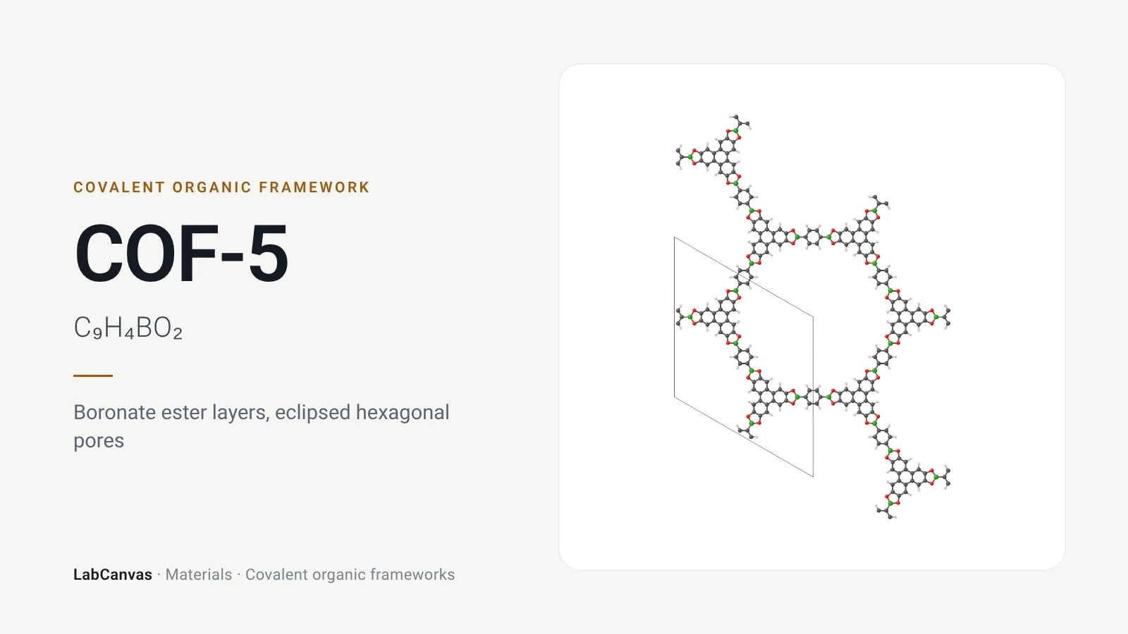
COF-5
COF-5, the boronate ester COF from HHTP and BDBA: eclipsed layers, 27 Å channels, 1,590 m² g⁻¹, synthesis and stability, with 2D and 3D figures to edit.
More on LabCanvas
- Dirac physics of graphene: Editable figure template
- Making graphene: six routes compared: Editable figure template
- Reading a graphene Raman spectrum: Editable figure template
- More figure templates in this category: Ready-made, cited figures to edit
- Crystal structure figure software compared: VESTA, Mercury, CrystalMaker, Avogadro and LabCanvas
- XRD Scherrer crystallite size calculator: Free tool
- Molar mass calculator: Free tool
- Journal figure size guide: Column widths and resolutions for 38 journals
- 3D models gallery: Turn MOFs, COFs and more in 3D
Frequently asked questions
What is graphene?
Graphene is a single layer of carbon atoms arranged in a flat honeycomb lattice, one atom thick. It is the building block of graphite and was first isolated in 2004 by Novoselov, Geim and co-workers, who peeled it from graphite with adhesive tape.
What is the structure of graphene?
A hexagonal (honeycomb) lattice of sp² carbon: each atom bonded to three neighbours 1.42 Å away, two atoms per unit cell, and a lattice constant of 2.46 Å. Stacked AB with 0.335 nm between layers, graphene sheets make graphite.
Is graphene a conductor?
Yes. Graphene is a semimetal with no band gap: its valence and conduction bands touch at the Dirac points, so it conducts electricity, and a gate voltage tunes the carriers from electrons to holes. The first devices had room-temperature mobilities of about 10,000 cm²/V·s (Novoselov et al., Science 2004).
Does graphene have a band gap?
No, pristine single-layer graphene has a zero band gap. A gap can be opened in bilayer graphene by an electric field between the layers (Zhang et al., Nature 2009).
How strong is graphene?
Nanoindentation of suspended sheets gave a Young’s modulus of 1.0 TPa and an intrinsic strength of 130 GPa, making graphene the strongest material ever measured at the time (Lee et al., Science 2008).
How thick is graphene?
One carbon atom. In graphite the layers are 0.335 nm apart, which is the thickness usually assigned to one sheet.
How is graphene made?
By peeling graphite with tape (mechanical exfoliation), by exfoliating graphite in liquids, by oxidising graphite to graphene oxide and reducing it, by chemical vapour deposition on copper foil, by heating silicon carbide, or by flash Joule heating of cheap carbon.
What is the difference between graphene and graphite?
Graphite is a stack of graphene sheets (AB-stacked, space group P6₃/mmc) held together by weak van der Waals forces. Graphene is one of those sheets on its own, with properties, such as its Dirac bands and half-integer quantum Hall effect, that the bulk crystal does not show.
How can I draw graphene for a paper or presentation?
Open the graphene figures on this page in LabCanvas (free), add the editable honeycomb drawing from the figure editor’s Library, open the graphite crystal structure, or open the 3D model in the LabCanvas 3D Studio and export a render.
References
- K. S. Novoselov, A. K. Geim, S. V. Morozov, D. Jiang, Y. Zhang, S. V. Dubonos, I. V. Grigorieva, A. A. Firsov. Electric field effect in atomically thin carbon films. Science 2004, 306, 666–669. doi:10.1126/science.1102896
- A. H. Castro Neto et al.. The electronic properties of graphene. Rev. Mod. Phys. 2009, 81, 109. doi:10.1103/RevModPhys.81.109
- P. R. Wallace. The band theory of graphite. Phys. Rev. 1947, 71, 622. doi:10.1103/PhysRev.71.622
- K. S. Novoselov et al.. Two-dimensional gas of massless Dirac fermions in graphene. Nature 2005, 438, 197. doi:10.1038/nature04233
- Y. Zhang et al.. Experimental observation of the quantum Hall effect and Berry’s phase in graphene. Nature 2005, 438, 201. doi:10.1038/nature04235
- C. Lee, X. Wei, J. W. Kysar, J. Hone. Measurement of the elastic properties and intrinsic strength of monolayer graphene. Science 2008, 321, 385–388. doi:10.1126/science.1157996
- A. A. Balandin et al.. Superior thermal conductivity of single-layer graphene. Nano Lett. 2008, 8, 902. doi:10.1021/nl0731872
- R. R. Nair et al.. Fine structure constant defines visual transparency of graphene. Science 2008, 320, 1308. doi:10.1126/science.1156965
- J. S. Bunch et al.. Impermeable atomic membranes from graphene sheets. Nano Lett. 2008, 8, 2458. doi:10.1021/nl801457b
- C. R. Dean et al.. Boron nitride substrates for high-quality graphene electronics. Nat. Nanotechnol. 2010, 5, 722–726. doi:10.1038/nnano.2010.172
- Y. Zhang et al.. Direct observation of a widely tunable bandgap in bilayer graphene. Nature 2009, 459, 820. doi:10.1038/nature08105
- Y. Sun et al.. Comparison of reduction products from graphite oxide and graphene oxide for anode applications in lithium-ion batteries and sodium-ion batteries. Nanoscale 2017, 9, 2585. doi:10.1039/c6nr07650e
- Y. Hernandez et al.. High-yield production of graphene by liquid-phase exfoliation of graphite. Nat. Nanotechnol. 2008, 3, 563. doi:10.1038/nnano.2008.215
- K. R. Paton et al.. Scalable production of large quantities of defect-free few-layer graphene by shear exfoliation in liquids. Nat. Mater. 2014, 13, 624. doi:10.1038/nmat3944
- W. S. Hummers, R. E. Offeman. Preparation of graphitic oxide. J. Am. Chem. Soc. 1958, 80, 1339. doi:10.1021/ja01539a017
- X. Li et al.. Large-area synthesis of high-quality and uniform graphene films on copper foils. Science 2009, 324, 1312. doi:10.1126/science.1171245
- S. Bae et al.. Roll-to-roll production of 30-inch graphene films for transparent electrodes. Nat. Nanotechnol. 2010, 5, 574. doi:10.1038/nnano.2010.132
- K. V. Emtsev et al.. Towards wafer-size graphene layers by atmospheric pressure graphitization of silicon carbide. Nat. Mater. 2009, 8, 203. doi:10.1038/nmat2382
- D. X. Luong et al.. Gram-scale bottom-up flash graphene synthesis. Nature 2020, 577, 647. doi:10.1038/s41586-020-1938-0
- S. Stankovich et al.. Graphene-based composite materials. Nature 2006, 442, 282. doi:10.1038/nature04969
- R. K. Joshi et al.. Precise and ultrafast molecular sieving through graphene oxide membranes. Science 2014, 343, 752. doi:10.1126/science.1245711
- A. C. Ferrari et al.. Raman spectrum of graphene and graphene layers. Phys. Rev. Lett. 2006, 97, 187401. doi:10.1103/PhysRevLett.97.187401
- J. A. Muñoz-Vargas et al.. Simple graphene film production by chemical vapour deposition and the use of AI for quality analysis. Nanoscale Adv. 2025, 7, 7382. doi:10.1039/d5na00668f
- A. K. Geim, I. V. Grigorieva. Van der Waals heterostructures. Nature 2013, 499, 419. doi:10.1038/nature12385
- Y. Cao et al.. Unconventional superconductivity in magic-angle graphene superlattices. Nature 2018, 556, 43–50. doi:10.1038/nature26160
- K. F. Mak et al.. Atomically thin MoS₂: a new direct-gap semiconductor. Phys. Rev. Lett. 2010, 105, 136805. doi:10.1103/PhysRevLett.105.136805
- B. Radisavljevic et al.. Single-layer MoS₂ transistors. Nat. Nanotechnol. 2011, 6, 147. doi:10.1038/nnano.2010.279
- K. Watanabe, T. Taniguchi, H. Kanda. Direct-bandgap properties and evidence for ultraviolet lasing of hexagonal boron nitride single crystal. Nat. Mater. 2004, 3, 404–409. doi:10.1038/nmat1134
- X. Liu et al.. Influence of hexagonal boron nitride on electronic structure of graphene. Molecules 2022, 27, 3740. doi:10.3390/molecules27123740
- M. Naguib et al.. Two-dimensional nanocrystals produced by exfoliation of Ti₃AlC₂. Adv. Mater. 2011, 23, 4248–4253. doi:10.1002/adma.201102306
Draw Graphene for your paper or slides
LabCanvas is a browser workspace for scientific figures: framework clusters, linkers and nets, crystal structures in 2D and 3D, graphs and posters, all editable.
Edit the Graphene figure