2D (layered) halide perovskites: Ruddlesden–Popper, Dion–Jacobson and the n value
Two-dimensional (2D), or layered, halide perovskites are slabs of corner-sharing lead halide octahedra, n layers thick, separated by bulky organic spacer cations; in the Ruddlesden–Popper series (BA)₂(MA)ₙ₋₁PbₙI₃ₙ₊₁ the band gap falls from 2.24 eV at n = 1 towards the 1.52 eV of MAPbI₃ as n grows (Cao et al. 2015). Each slab acts as a natural quantum well holding tightly bound excitons (Blancon et al. 2018). In 2014 Smith et al. used the phenethylammonium phase (PEA)₂(MA)₂Pb₃I₁₀ as a more moisture-resistant solar absorber, and in 2016 Tsai et al. raised layered perovskite cells to 12.52%.
Contents
2D perovskites at a glance
| Formula (Ruddlesden–Popper) | A′₂Aₙ₋₁BₙX₃ₙ₊₁, e.g. (BA)₂(MA)ₙ₋₁PbₙI₃ₙ₊₁ with BA = butylammonium, MA = methylammonium (Cao et al. 2015; Blancon et al. 2018) |
|---|---|
| Formula (Dion–Jacobson) | A′Aₙ₋₁PbₙI₃ₙ₊₁ with one A′ per formula unit, e.g. A′ = 3- or 4-(aminomethyl)piperidinium (Mao et al. 2018) |
| n | Number of octahedral layers per inorganic slab; n = ∞ is the 3D perovskite (Cao et al. 2015) |
| Slab thickness | 0.641 nm (n = 1) to 3.139 nm (n = 5) in (BA)₂(MA)ₙ₋₁PbₙI₃ₙ₊₁ (Blancon et al. 2018) |
| Band gap vs n | Falls with n: 2.24 eV for (BA)₂PbI₄ to 1.52 eV for MAPbI₃ in films (Cao et al. 2015) |
| Exciton binding energy | 470 meV (n = 1) to 125 meV (n = 5) (Blancon et al. 2018) |
| Dielectric contrast | Dielectric constant about 4–5.2 in the perovskite layers vs about 2.2 in the organic spacers, from DFT (Blancon et al. 2018) |
| Spacer cations | Butylammonium (Cao et al. 2015), phenethylammonium (Smith et al. 2014), 3AMP and 4AMP (Dion–Jacobson; Mao et al. 2018) |
| Early 2D absorber cell | (PEA)₂(MA)₂Pb₃I₁₀: Voc 1.18 V, 4.73%, films more moisture resistant than MAPbI₃ (Smith et al. 2014) |
| RP solar cells | 4.02% for n = 3 BA phase (Cao et al. 2015); 12.52% with no hysteresis from near-single-crystalline, vertically aligned films (Tsai et al. 2016) |
| DJ solar cells | 7.32% for the best 3AMP-based member, much higher than its 4AMP analogue (Mao et al. 2018) |
| Stability | Unencapsulated 2D cells kept over 60% of their efficiency for over 2,250 h under AM1.5G light and tolerated 65% relative humidity better than 3D cells (Tsai et al. 2016) |
| LEDs | Near-infrared LEDs from quantum-size-tuned grains: EQE 8.8%, radiance 80 W sr⁻¹ m⁻² (Yuan et al. 2016) |
| Key reports | Smith et al., Angew. Chem. Int. Ed. 53, 11232 (2014); Cao et al., J. Am. Chem. Soc. 137, 7843 (2015); Tsai et al., Nature 536, 312 (2016) |
2D perovskites in 3D (interactive)
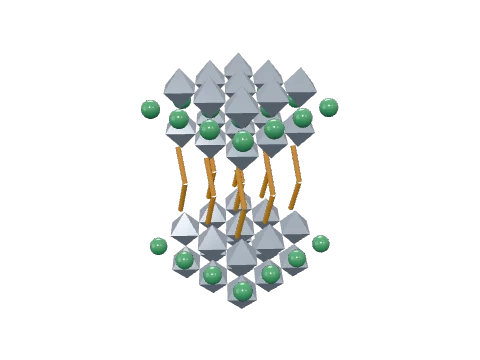
Loading the 3D model…
2D perovskite structure explained
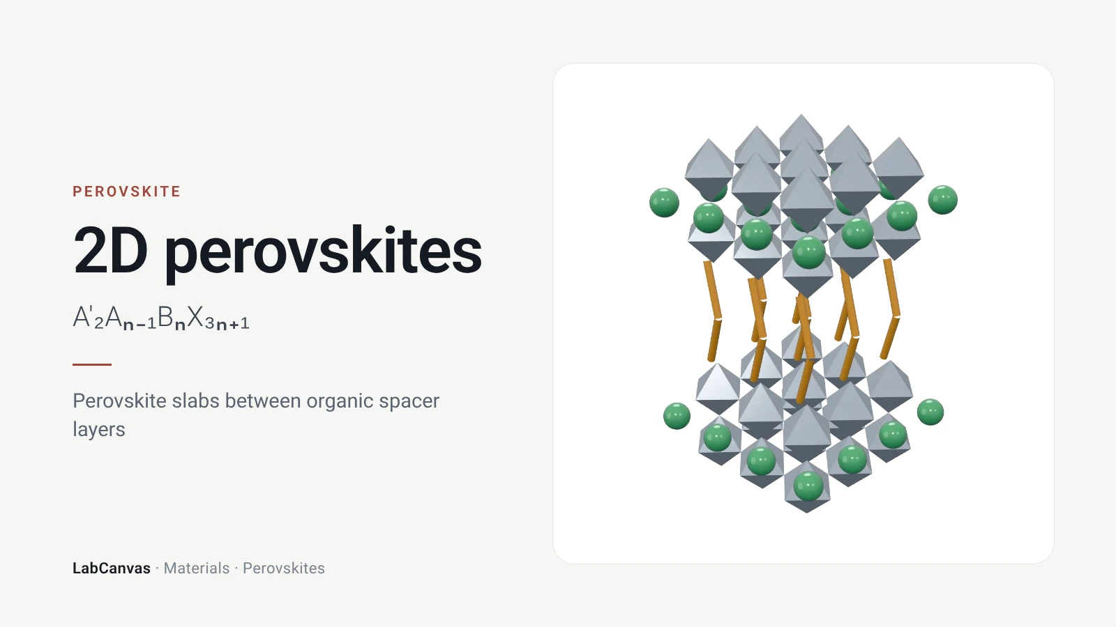
A 3D halide perovskite such as MAPbI₃ is an endless framework of corner-sharing PbI₆ octahedra with a small cation in every cage (see the perovskite structure hub). Cut that framework into slabs n octahedra thick and fill the gaps with cations too large to fit in the cages, and you have a 2D (layered) perovskite. The formula of the butylammonium series, (BA)₂(MA)ₙ₋₁PbₙI₃ₙ₊₁, shows the parts: two bulky butylammonium (BA) spacers, n − 1 methylammonium (MA) ions inside the slab, and n layers of PbI₆ octahedra (Cao et al. 2015). Phase-pure members from n = 1 to n = 5 have slabs 0.641 to 3.139 nm thick (Blancon et al. 2018), and n = ∞ is MAPbI₃ itself (Cao et al. 2015). These layered compounds belong to the wider family of organic–inorganic perovskites, which spans 3D and lower-dimensional structures (Saparov & Mitzi 2016).
The integer n sets the thickness of the inorganic layer, and phase-pure crystals with a single n value up to n = 5 have been synthesised (Blancon et al. 2018).
Ruddlesden–Popper vs Dion–Jacobson phases
- Ruddlesden–Popper (RP). General formula A′₂Aₙ₋₁BₙX₃ₙ₊₁: two spacer cations A′ per formula unit, such as butylammonium (Cao et al. 2015; Blancon et al. 2018) or phenethylammonium (Smith et al. 2014).
- Dion–Jacobson (DJ). General formula A′Aₙ₋₁PbₙI₃ₙ₊₁: one spacer A′ per formula unit, so the spacer must carry a 2+ charge (from the charge balance of the formula). Mao et al. (2018) reported the first complete homologous DJ series in halide perovskites, with 3-(aminomethyl)piperidinium (3AMP) or 4-(aminomethyl)piperidinium (4AMP) as A′; their inorganic layers lie exactly on top of one another. Moving the aminomethyl group from the 4- to the 3-position gives smaller band gaps.
Quantum and dielectric confinement
Each inorganic slab is a natural quantum well: the electron and hole wavefunctions stay in the perovskite layer with little leakage into the organic spacers (Blancon et al. 2018). Two effects follow.
- Quantum confinement widens the band gap as the slab thins: in the BA series it rises from 1.52 eV for MAPbI₃ to 2.24 eV for n = 1 (Cao et al. 2015).
- Dielectric confinement strengthens the electron–hole attraction, because the organic spacers (dielectric constant about 2.2) screen it less than the perovskite (about 4–5.2). Together the two give exciton binding energies of 470 meV at n = 1 falling to 125 meV at n = 5, with dielectric confinement dominating in the thinnest slabs (Blancon et al. 2018). Excitons are predicted to stay bound above room-temperature thermal energy up to n ≈ 20, a slab about 12.6 nm thick (Blancon et al. 2018).
2D perovskite solar cells and moisture stability
3D MAPbI₃ is unstable to moisture and needs anhydrous processing (Smith et al. 2014). Smith et al. (2014) used the n = 3 phenethylammonium phase (PEA)₂(MA)₂Pb₃I₁₀ as the absorber: its films were more moisture resistant than MAPbI₃, devices could be made at ambient humidity, and the cells gave an open-circuit voltage of 1.18 V and 4.73%. Cao et al. (2015) made cells from the (BA)₂(MA)ₙ₋₁PbₙI₃ₙ₊₁ series; the n = 3 compound gave 4.02% and kept its performance after long exposure to high humidity, and the films self-assembled with the inorganic layers perpendicular to the substrate.
The low efficiency came from the organic spacers acting as insulating layers that block out-of-plane charge transport. Tsai et al. (2016) overcame this with near-single-crystalline films whose inorganic planes are aligned out-of-plane, reaching 12.52% with no hysteresis; unencapsulated cells kept over 60% of their efficiency for over 2,250 hours under constant illumination and tolerated 65% relative humidity better than 3D cells, and encapsulated cells showed no degradation. Dion–Jacobson phases have also been used as absorbers, with 7.32% for the best 3AMP-based compound (Mao et al. 2018).
2D perovskite LEDs
Confinement also helps light emission. Yuan et al. (2016) made a mixed material of grains with different quantum-size-tuned gaps that funnels excitations to the lowest-gap emitter, so radiative recombination outcompetes trapping; their near-infrared LEDs reached an external quantum efficiency of 8.8% and a radiance of 80 W sr⁻¹ m⁻².
How to draw the 2D perovskite structure
For a paper, slide or poster, draw the slabs side on: n layers of corner-sharing octahedra, then a layer of spacer cations, repeated. Showing n = 1, 2 and 3 next to the 3D (n = ∞) framework makes the n value obvious, and a schematic band diagram of wide-gap organic barriers and narrow-gap perovskite wells explains the confinement. For a Dion–Jacobson phase, draw a single doubly charged spacer layer between adjacent slabs, with the slabs directly above one another. In the LabCanvas figure editor, the Library’s Perovskite crystal object draws corner-sharing octahedra that you can stack into slabs, add spacer molecules to, recolour and export as a high-resolution SVG; the perovskite structure page shows the 3D framework the slabs are cut from.
Ruddlesden–Popper vs Dion–Jacobson vs 3D perovskites
| Type | General formula | Spacer per formula unit | Example | Band gap | Solar cell report |
|---|---|---|---|---|---|
| Ruddlesden–Popper | A′₂Aₙ₋₁PbₙI₃ₙ₊₁ | Two (e.g. butylammonium, phenethylammonium) | (BA)₂(MA)ₙ₋₁PbₙI₃ₙ₊₁ | 2.24 eV (n = 1), falling with n | 4.73% (Smith et al. 2014); 12.52% (Tsai et al. 2016) |
| Dion–Jacobson | A′Aₙ₋₁PbₙI₃ₙ₊₁ | One 2+ cation (e.g. 3AMP, 4AMP) | (3AMP)(MA)ₙ₋₁PbₙI₃ₙ₊₁ | 3AMP series smaller than 4AMP series | 7.32% (Mao et al. 2018) |
| 3D (n = ∞) | APbI₃ | None | MAPbI₃ | 1.52 eV | 3.8% as a sensitiser (Kojima et al. 2009) |
Related materials
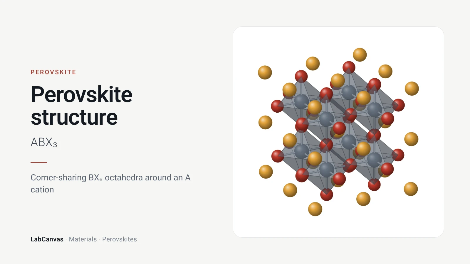
Perovskite structure
The perovskite structure explained: ABX₃ with corner-sharing BX₆ octahedra, the tolerance factor, octahedral tilts, and oxide vs halide perovskites.
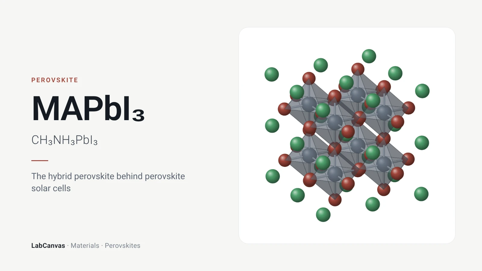
MAPbI₃
MAPbI₃ (CH₃NH₃PbI₃): tetragonal and cubic phases, 1.5 eV band gap, the first perovskite solar cells, long diffusion lengths, instability and lead toxicity.
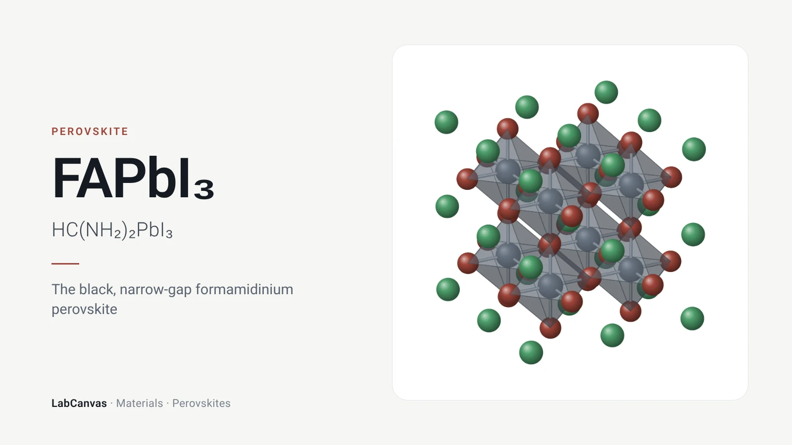
FAPbI₃
FAPbI₃ explained: the black cubic α-phase and yellow hexagonal δ-phase, its 1.48 eV band gap, how mixed cations stabilise it and its role in solar cells.
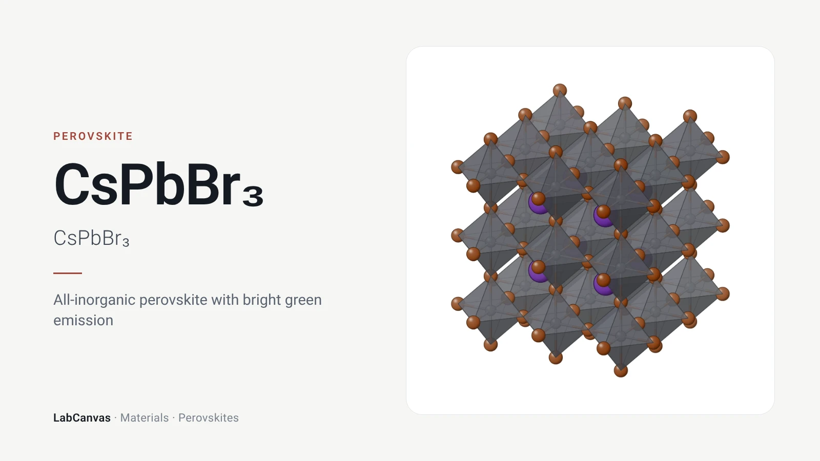
CsPbBr₃
CsPbBr₃ and CsPbX₃ perovskite quantum dots: orthorhombic structure, hot-injection synthesis, emission tunable over 410–700 nm, anion exchange and uses.
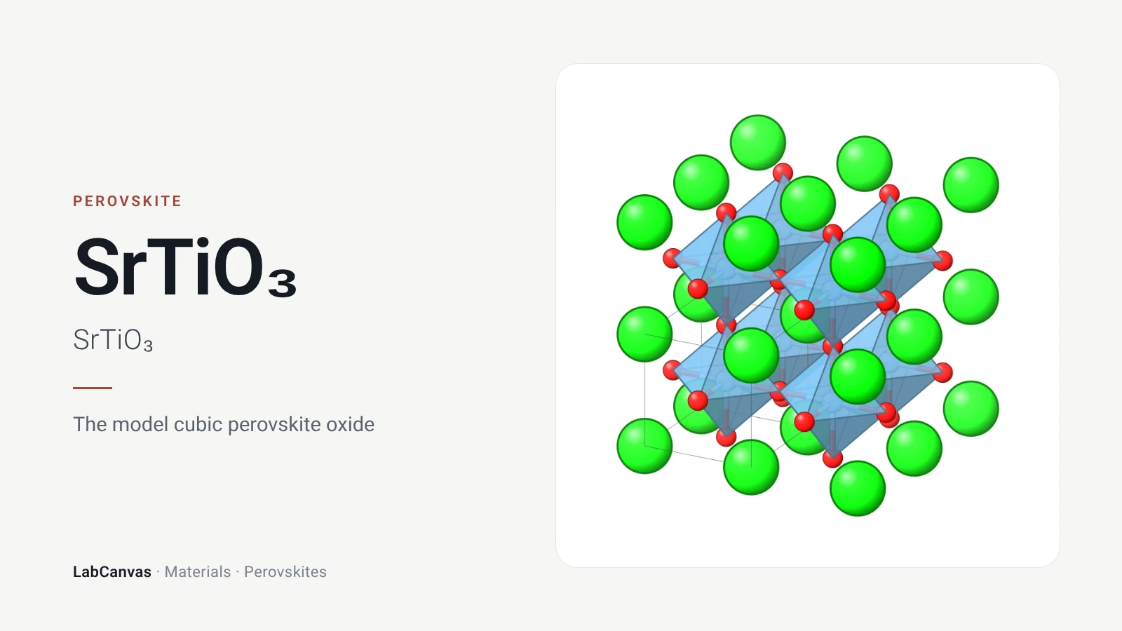
SrTiO₃ (strontium titanate)
SrTiO₃ structure and properties: cubic perovskite (a = 3.905 Å), the 105 K transition, quantum paraelectricity, LaAlO₃/SrTiO₃ interfaces and water splitting.
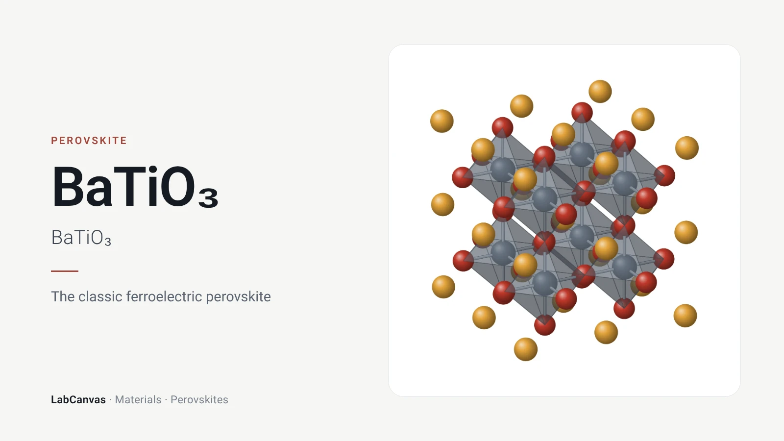
BaTiO₃ (barium titanate)
BaTiO₃, the classic ferroelectric perovskite: its ~120 °C Curie point, tetragonal, orthorhombic and rhombohedral phases, capacitors and piezoelectrics.
More on LabCanvas
- Crystal structure figure software compared: VESTA, Mercury, CrystalMaker, Avogadro and LabCanvas
- Tauc plot band gap calculator: Free tool: optical band gap from UV–vis
- XRD Scherrer crystallite size calculator: Free tool
- Molar mass calculator: Free tool
- Journal figure size guide: Column widths and resolutions for 38 journals
- 3D models gallery: Turn MOFs, COFs, perovskites and more in 3D
Frequently asked questions
What is a 2D perovskite?
A layered halide perovskite: slabs of corner-sharing metal halide octahedra, n layers thick, separated by bulky organic spacer cations, e.g. (BA)₂(MA)ₙ₋₁PbₙI₃ₙ₊₁ (Cao et al. 2015). Each slab behaves as a natural quantum well (Blancon et al. 2018).
What is a Ruddlesden–Popper perovskite?
A layered perovskite with the formula A′₂Aₙ₋₁BₙX₃ₙ₊₁, two spacer cations A′ per formula unit, such as butylammonium in (BA)₂(MA)ₙ₋₁PbₙI₃ₙ₊₁ (Cao et al. 2015; Blancon et al. 2018).
What is the difference between Ruddlesden–Popper and Dion–Jacobson perovskites?
Ruddlesden–Popper phases have two spacer cations per formula unit (A′₂Aₙ₋₁BₙX₃ₙ₊₁); Dion–Jacobson phases have one doubly charged spacer (A′Aₙ₋₁PbₙI₃ₙ₊₁), and in the lead iodide DJ series of Mao et al. (2018) the inorganic layers lie exactly on top of one another.
What does n mean in 2D perovskites?
The number of octahedral layers in each inorganic slab. n = 1 is a single layer of octahedra between spacers; as n grows the slab thickens (0.641 nm at n = 1 to 3.139 nm at n = 5; Blancon et al. 2018) and the material approaches the 3D perovskite, n = ∞.
How does the band gap of 2D perovskites change with n?
It falls as n increases: in (BA)₂(MA)ₙ₋₁PbₙI₃ₙ₊₁ films from 2.24 eV at n = 1 to 1.52 eV for MAPbI₃ (Cao et al. 2015). The exciton binding energy also falls, from 470 meV at n = 1 to 125 meV at n = 5 (Blancon et al. 2018).
Why are 2D perovskites more stable than 3D perovskites?
The bulky organic spacers make the films more resistant to moisture: (PEA)₂(MA)₂Pb₃I₁₀ films resisted moisture better than MAPbI₃ (Smith et al. 2014), and 2D Ruddlesden–Popper cells kept over 60% of their efficiency for 2,250 h of illumination unencapsulated and tolerated 65% humidity better than 3D cells (Tsai et al. 2016).
What is the efficiency of 2D perovskite solar cells?
The first layered-perovskite absorber cells gave 4.73% (Smith et al. 2014) and 4.02% (Cao et al. 2015); aligning the slabs vertically raised this to 12.52% (Tsai et al., Nature 2016). A Dion–Jacobson absorber gave 7.32% (Mao et al. 2018).
Are 2D perovskites used in LEDs?
Yes. Mixtures of quantum-size-tuned perovskite grains funnel excitations to the lowest-gap emitter, giving near-infrared LEDs with 8.8% external quantum efficiency and a radiance of 80 W sr⁻¹ m⁻² (Yuan et al. 2016).
References
- I. C. Smith, E. T. Hoke, D. Solis-Ibarra, M. D. McGehee, H. I. Karunadasa. A layered hybrid perovskite solar-cell absorber with enhanced moisture stability. Angew. Chem. Int. Ed. 2014, 53, 11232–11235. doi:10.1002/anie.201406466
- D. H. Cao, C. C. Stoumpos, O. K. Farha, J. T. Hupp, M. G. Kanatzidis. 2D homologous perovskites as light-absorbing materials for solar cell applications. J. Am. Chem. Soc. 2015, 137, 7843–7850. doi:10.1021/jacs.5b03796
- H. Tsai et al.. High-efficiency two-dimensional Ruddlesden–Popper perovskite solar cells. Nature 2016, 536, 312–316. doi:10.1038/nature18306
- L. Mao et al.. Hybrid Dion–Jacobson 2D lead iodide perovskites. J. Am. Chem. Soc. 2018, 140, 3775–3783. doi:10.1021/jacs.8b00542
- J.-C. Blancon et al.. Scaling law for excitons in 2D perovskite quantum wells. Nat. Commun. 2018, 9, 2254. doi:10.1038/s41467-018-04659-x
- M. Yuan et al.. Perovskite energy funnels for efficient light-emitting diodes. Nat. Nanotechnol. 2016, 11, 872–877. doi:10.1038/nnano.2016.110
- B. Saparov, D. B. Mitzi. Organic–inorganic perovskites: structural versatility for functional materials design. Chem. Rev. 2016, 116, 4558–4596. doi:10.1021/acs.chemrev.5b00715
- A. Kojima, K. Teshima, Y. Shirai, T. Miyasaka. Organometal halide perovskites as visible-light sensitizers for photovoltaic cells. J. Am. Chem. Soc. 2009, 131, 6050–6051. doi:10.1021/ja809598r
Draw 2D perovskites for your paper or slides
LabCanvas is a browser workspace for scientific figures: framework clusters, linkers and nets, crystal structures in 2D and 3D, graphs and posters, all editable.
Draw 2D perovskites in LabCanvas