Graphical abstract template · Graphical abstracts · Graphical abstract
Hexagonal boron nitride: the floor, the sandwich and the light
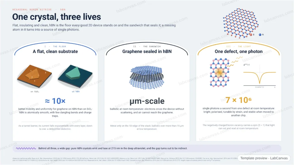
A triptych of hBN’s three roles: an atomically flat, trap-free dielectric that makes graphene almost ten times better than on SiO₂; the encapsulating sandwich that keeps graphene ballistic over micrometres at room temperature; and atomic defects that emit single photons at room temperature, some with optically addressable spins. A strip at the foot adds the wide gap behind it all, with deep-ultraviolet emission at 215 nm.
Updated 9 cited papers54 editable layers
At a glance
- Category
- Graphical abstracts
- Method
- Graphical abstract
- Starting materials
- Hexagonal boron nitride crystals, exfoliated to flakes down to one layer
- Product
- Dielectric substrates, encapsulating layers, tunnel barriers and quantum emitters
- Key result
- ≈ 10× better mobility than on SiO₂ (Dean et al. 2010); ballistic > 15 µm (Wang et al. 2013); > 7 × 10⁶ photons s⁻¹ (Grosso et al. 2017); 215 nm emission (Watanabe et al. 2004)
- Figure
- 1920 × 1080 px (16:9), 54 editable layers, 3 generated objects
Step by step
- The floorAtomically smooth, with few dangling bonds and charge traps: graphene on h-BN has mobility and inhomogeneity almost 10× better than on SiO₂ (Dean et al. 2010); a defect-free tunnel barrier down to one layer (Britnell et al. 2012)
- The sandwichEncapsulated graphene is ballistic over micrometres at room temperature and shielded from air (Mayorov et al. 2011); with 1D edge contacts, over > 15 µm at low temperature (Wang et al. 2013)
- The lightRoom-temperature, polarised, ultrabright single-photon emission from a defect (Tran et al. 2016); strain tuning over 6 meV and > 7 × 10⁶ counts s⁻¹ (Grosso et al. 2017); the negatively charged boron vacancy shows ODMR at room temperature (Gottscholl et al. 2020)
- The gapLuminescence and lasing at 215 nm (Watanabe et al. 2004), from an indirect band gap (Cassabois et al. 2016)
Uses
- Graphical abstracts on hBN and 2D dielectrics
- Talks on encapsulated 2D devices and quantum emitters in van der Waals crystals
- Teaching why the substrate matters for 2D electronics
Papers this template follows
- Dean et al., “Boron nitride substrates for high-quality graphene electronics”, Nat. Nanotechnol. 2010. doi:10.1038/nnano.2010.172primary
- Britnell et al., “Electron tunneling through ultrathin boron nitride crystalline barriers”, Nano Lett. 2012. doi:10.1021/nl3002205primary
- Mayorov et al., “Micrometer-scale ballistic transport in encapsulated graphene at room temperature”, Nano Lett. 2011. doi:10.1021/nl200758bprimary
- Wang et al., “One-dimensional electrical contact to a two-dimensional material”, Science 2013. doi:10.1126/science.1244358primary
- Tran et al., “Quantum emission from hexagonal boron nitride monolayers”, Nat. Nanotechnol. 2016. doi:10.1038/nnano.2015.242primary
- Grosso et al., “Tunable and high-purity room temperature single-photon emission from atomic defects in hexagonal boron nitride”, Nat. Commun. 2017. doi:10.1038/s41467-017-00810-2primary
- Gottscholl et al., “Initialization and read-out of intrinsic spin defects in a van der Waals crystal at room temperature”, Nat. Mater. 2020. doi:10.1038/s41563-020-0619-6primary
- Watanabe, Taniguchi & Kanda, “Direct-bandgap properties and evidence for ultraviolet lasing of hexagonal boron nitride single crystal”, Nat. Mater. 2004. doi:10.1038/nmat1134primary
- Cassabois, Valvin & Gil, “Hexagonal boron nitride is an indirect bandgap semiconductor”, Nat. Photonics 2016. doi:10.1038/nphoton.2015.277primary
Drawn by LabCanvas after Dean et al., Nat. Nanotechnol. 2010 (doi:10.1038/nnano.2010.172); Britnell et al., Nano Lett. 2012 (doi:10.1021/nl3002205); Mayorov et al., Nano Lett. 2011 (doi:10.1021/nl200758b); Wang et al., Science 2013 (doi:10.1126/science.1244358); Tran et al., Nat. Nanotechnol. 2016 (doi:10.1038/nnano.2015.242); Grosso et al., Nat. Commun. 2017 (doi:10.1038/s41467-017-00810-2); Gottscholl et al., Nat. Mater. 2020 (doi:10.1038/s41563-020-0619-6); Watanabe et al., Nat. Mater. 2004 (doi:10.1038/nmat1134); Cassabois et al., Nat. Photonics 2016 (doi:10.1038/nphoton.2015.277). Height maps simulated; photon train and g⁽²⁾ schematic.
How templates are written and checked: editorial guidelines.
Questions
What does the “Hexagonal boron nitride: the floor, the sandwich and the light” template show?
A triptych of hBN’s three roles: an atomically flat, trap-free dielectric that makes graphene almost ten times better than on SiO₂; the encapsulating sandwich that keeps graphene ballistic over micrometres at room temperature; and atomic defects that emit single photons at room temperature, some with optically addressable spins. A strip at the foot adds the wide gap behind it all, with deep-ultraviolet emission at 215 nm.
What are the steps shown in “Hexagonal boron nitride: the floor, the sandwich and the light”?
1. The floor: Atomically smooth, with few dangling bonds and charge traps: graphene on h-BN has mobility and inhomogeneity almost 10× better than on SiO₂ (Dean et al. 2010); a defect-free tunnel barrier down to one layer (Britnell et al. 2012). 2. The sandwich: Encapsulated graphene is ballistic over micrometres at room temperature and shielded from air (Mayorov et al. 2011); with 1D edge contacts, over > 15 µm at low temperature (Wang et al. 2013). 3. The light: Room-temperature, polarised, ultrabright single-photon emission from a defect (Tran et al. 2016); strain tuning over 6 meV and > 7 × 10⁶ counts s⁻¹ (Grosso et al. 2017); the negatively charged boron vacancy shows ODMR at room temperature (Gottscholl et al. 2020). 4. The gap: Luminescence and lasing at 215 nm (Watanabe et al. 2004), from an indirect band gap (Cassabois et al. 2016).
What are the starting materials and the product?
Starting materials: Hexagonal boron nitride crystals, exfoliated to flakes down to one layer. Product: Dielectric substrates, encapsulating layers, tunnel barriers and quantum emitters.
Which papers is “Hexagonal boron nitride: the floor, the sandwich and the light” based on?
Dean et al., “Boron nitride substrates for high-quality graphene electronics”, Nat. Nanotechnol. 2010 (doi:10.1038/nnano.2010.172); Britnell et al., “Electron tunneling through ultrathin boron nitride crystalline barriers”, Nano Lett. 2012 (doi:10.1021/nl3002205); Mayorov et al., “Micrometer-scale ballistic transport in encapsulated graphene at room temperature”, Nano Lett. 2011 (doi:10.1021/nl200758b); Wang et al., “One-dimensional electrical contact to a two-dimensional material”, Science 2013 (doi:10.1126/science.1244358); Tran et al., “Quantum emission from hexagonal boron nitride monolayers”, Nat. Nanotechnol. 2016 (doi:10.1038/nnano.2015.242); Grosso et al., “Tunable and high-purity room temperature single-photon emission from atomic defects in hexagonal boron nitride”, Nat. Commun. 2017 (doi:10.1038/s41467-017-00810-2); Gottscholl et al., “Initialization and read-out of intrinsic spin defects in a van der Waals crystal at room temperature”, Nat. Mater. 2020 (doi:10.1038/s41563-020-0619-6); Watanabe, Taniguchi & Kanda, “Direct-bandgap properties and evidence for ultraviolet lasing of hexagonal boron nitride single crystal”, Nat. Mater. 2004 (doi:10.1038/nmat1134); Cassabois, Valvin & Gil, “Hexagonal boron nitride is an indirect bandgap semiconductor”, Nat. Photonics 2016 (doi:10.1038/nphoton.2015.277).
Can I edit the “Hexagonal boron nitride: the floor, the sandwich and the light” template?
Yes. Open it in the LabCanvas editor: all 54 layers are editable, including 3 generated objects (structures, plots, equipment) with their own settings. Change the text, colours and layout, then export PNG, TIFF or PDF at the width and DPI the journal asks for.
Do I need an account to use this template?
Not to view it here. To open and edit it, sign in to LabCanvas or create a free account (the free plan keeps up to 3 designs). Downloading the figure is part of LabCanvas Pro (US$19 a month or US$199 a year).